Methods for forming silicon comprising films using hexachlorodisilane in a single-wafer deposion chamber

a technology of hexachlorodisilane and deposition chamber, which is applied in the direction of liquid surface applicators, chemical vapor deposition coatings, coatings, etc., can solve the problems of slow deposition rate, excessive by-product particle contamination, and inability to form uniform films

Inactive Publication Date: 2005-04-26
APPLIED MATERIALS INC
View PDF4 Cites 22 Cited by
  • Summary
  • Abstract
  • Description
  • Claims
  • Application Information

AI Technical Summary

Problems solved by technology

However, with many intricate, dense and complex structures of the components to be formed on the semiconductor device, it is becoming difficult to form uniform films with good step coverage using the current silane and disilane chemistry.
One disadvantage of current methods that utilize the hexachlorodisilane chemistry to form a silicon comprising film includes excessive by-product particle contamination that requires unnecessary and complicated cleaning as well as complicated efficient / exhaust management.
Another disadvantage includes slow deposition rate.
Further yet, current methods utilize batch processing type of chambers, which limit the rate of customizing and controlling film properties for any particular product.

Method used


Image

  • Methods for forming silicon comprising films using hexachlorodisilane in a single-wafer deposion chamber
  • Methods for forming silicon comprising films using hexachlorodisilane in a single-wafer deposion chamber
  • Methods for forming silicon comprising films using hexachlorodisilane in a single-wafer deposion chamber

Examples


Embodiment Construction

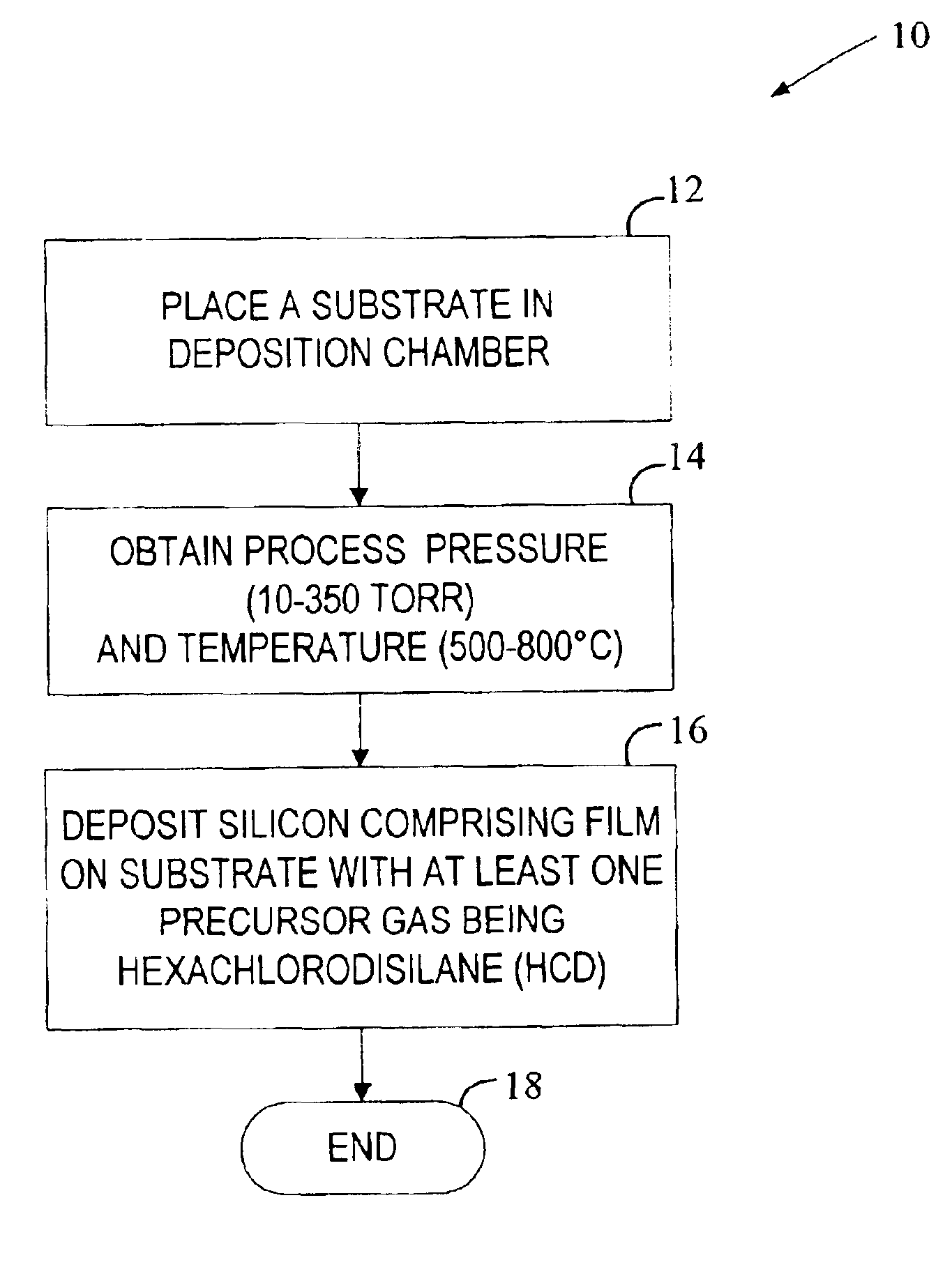
[0020]The present invention is a novel method of forming a silicon comprising film in a single-wafer deposition chamber using hexachlorodisilane precursor. In the following description, for purposes of explanation, numerous specific details are set forth in order to provide a thorough understanding of the present invention. It will be evident, however, to one skilled in the art that the present invention may be practiced without these specific details. In other instances, specific apparatus structures and methods have not been described so as not to obscure the present invention. The following description and drawings are illustrative of the invention and are not to be construed as limiting the invention.

[0021]Hexachlorodisilane is sometimes abbreviated as “HCD” throughout this discussion.

[0022]The following sections describe novel methods of forming silicon comprising film using HCD precursor in a single-wafer deposition chamber. The single-wafer deposition chamber can be a cold-wa...


PUM

PropertyMeasurementUnit
pressureaaaaaaaaaa
pressureaaaaaaaaaa
pressureaaaaaaaaaa

Abstract

A silicon comprising film and its method of fabrication is described. The silicon comprising film is grown on a substrate. A hexachlorodisilane (HCD) source gas is one of the reactant species used to form the silicon comprising film. The silicon comprising film is formed under a pressure between 10 Torr and 350 Torr.

Description

BACKGROUND OF THE INVENTION[0001]1. Field of the Invention[0002]The present invention relates to forming silicon comprising films for semiconductor devices and more specifically to forming the silicon comprising films using hexachlorodisilane as a precursor in a single-wafer deposition chamber.[0003]2. Discussion of Related Art[0004]Chemical vapor deposition (CVD) have been widely used to form silicon comprising films such as silicon oxide, silicon nitride, and silicon oxynitride. These films have wide applications in fabrication of integrated circuits such as transistors, microprocessors, and memories. These films are used as spacers, as etch stops, as diffusion and implantation masks, as capacitors, as dielectrics, as anti-reflection coatings, and as final passivation layers. Acceptable processes for making the silicon comprising films include those that form films with uniform thickness, uniform composition, low particulates, low chemical contamination, good adhesion to the subst...

Claims


Application Information

Patent Timeline
Patent Type & Authority Patents(United States)
IPC IPC(8): C23C16/30C23C16/40C23C16/22C23C16/24C23C16/34H01L21/205H01L21/318H01L21/02H01L21/314H01L21/316C23C16/44C23C16/455
CPCC23C16/24H01L21/02661C23C16/345C23C16/402C23C16/4411C23C16/45512H01L21/0214H01L21/02164H01L21/0217H01L21/022H01L21/02271H01L21/02337H01L21/3144H01L21/31612H01L21/3185H01L21/02381H01L21/0242H01L21/02422H01L21/02532H01L21/0262C23C16/308
Inventor LUO, LEEIYER, R. SURYANARAYANANSUBRAMONY, JANARDHANAN ANANDSANCHEZ, ERROL ANTONIO C.JIN, XIAOLIANGCHEN, AIHUAYAN, CHANG-LIANTOKAI, NOBUOMAEDA, YUJITHAKUR, RANDHIR P. SINGH
Owner APPLIED MATERIALS INC
Why Eureka
Try Eureka