Stiffened backside fabrication for microwave radio frequency wafers

a backside fabrication and microwave radio frequency technology, applied in the direction of electrical equipment, semiconductor devices, semiconductor/solid-state device details, etc., can solve the problems of excessive device performance loss, thinner wafers usually break, and processing of wafers usually stop, so as to achieve less damage susceptible and less fragile

Inactive Publication Date: 2005-04-26
SANDVIK AB +1
View PDF19 Cites 44 Cited by
  • Summary
  • Abstract
  • Description
  • Claims
  • Application Information

AI Technical Summary

Benefits of technology

[0005]The present invention provides a dry gas etching-based wafer thinning arrangement usable as an improved alternative to the usual grinding and polishing wafer thinning. In the present invention the wafer is provided with an array of backside support and rigidizing members enabling use of conventional wafer handling and processing notwithstanding its thinned and paper-like fragile nature. Selective backside etching of the wafer in the presence of both patterned and processing fixture-provided masking provides a residual array of interconnected backside support members which combine to make the wafer significantly less fragile and less damage susceptible in the whole wafer state than is possible with conventional thin wafer processes. The backside support members may be excluded in the wafer dicing operation where the accomplished small die size affords such die strength as to enable conventional die handing for packaging purposes.
[0006]It is therefore an object of the present invention to provide an improved integrated circuit wafer thinning process.
[0007]It is another object of the invention to provide a thinned integrated circuit wafer having enhanced breakage damage immunity.
[0019]each said recessed cavity region of said backside array being disposed in lateral registration with one of said frontal surface radio frequency electrical circuit die locations and comprising a region of diminished wafer thickness and enhanced electrical and thermal performance for components of said registered frontal surface radio frequency electrical circuit device;
[0020]each said recessed cavity region in said backside array being bounded by a pattern of plateau cross-sectioned wafer material disposed in both lateral registration with a periphery of each said circuit die and in rigidifying physical strengthening of said circuit die and said region of diminished semiconductor wafer thickness.

Problems solved by technology

Thinner wafers usually break during processing, at which point processing of the wafer usually stops because it is not cost effective to process wafer pieces of irregular shape in a production line.
For microwave frequency integrated circuit devices (usually circuits operable in the gigahertz frequency range such as Monolithic Microwave Integrated Circuits or MMIC's), the standard wafer thickness (e.g. 600 μm) is however too thick and thereby excessive device performance losses will occur.
Such wafers are usually thinned to 100 micrometers or even thinner, and require special handling during the backside operation and possibly during subsequent packaging, since the thinned wafers are so structurally weakened as to be quite fragile and unsound.
This dismounting procedure is undesirably critical, and frequently results in wafer breakage, as the wafer is now very thin and has become structurally unsound.

Method used


Image

  • Stiffened backside fabrication for microwave radio frequency wafers
  • Stiffened backside fabrication for microwave radio frequency wafers
  • Stiffened backside fabrication for microwave radio frequency wafers

Examples


Embodiment Construction

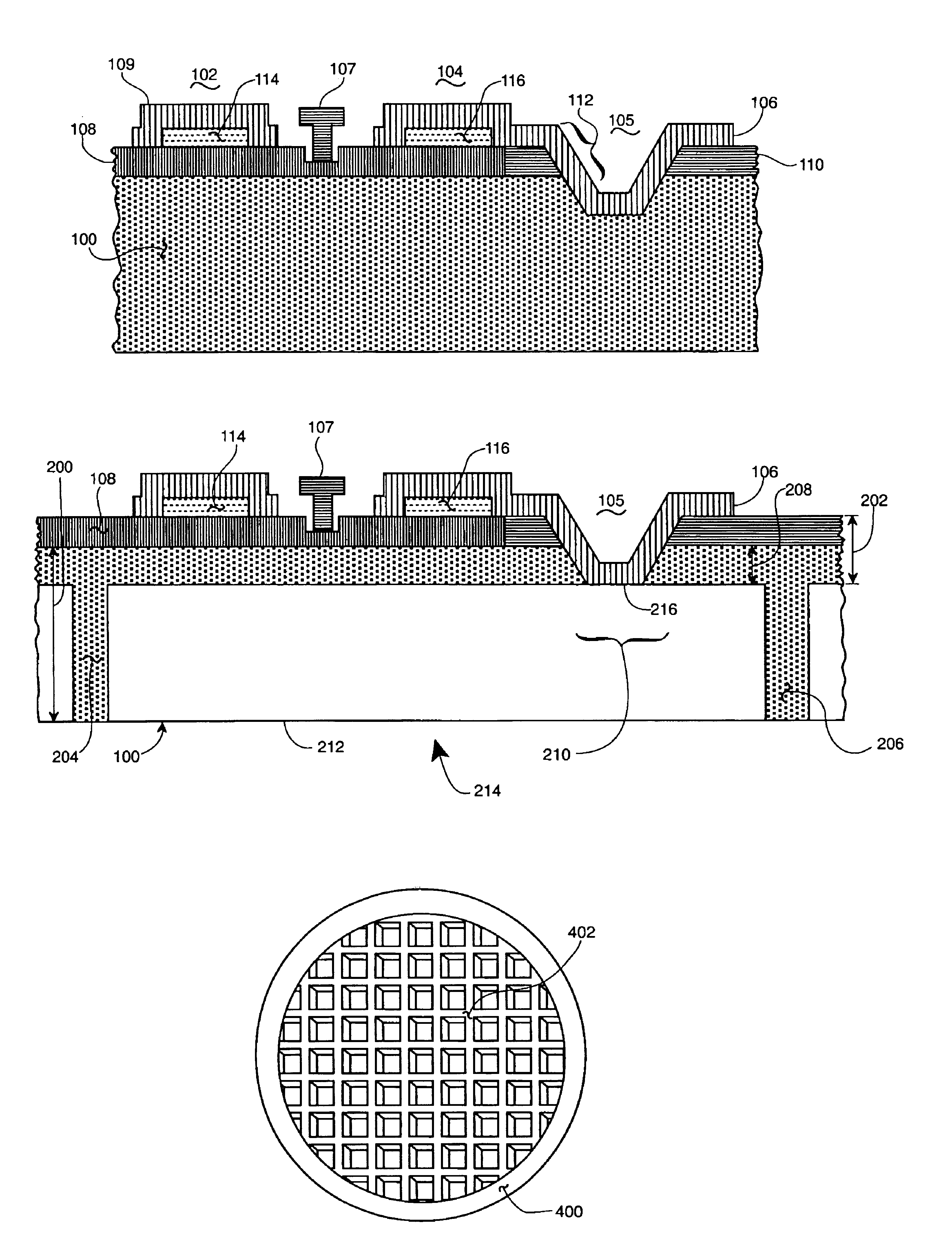
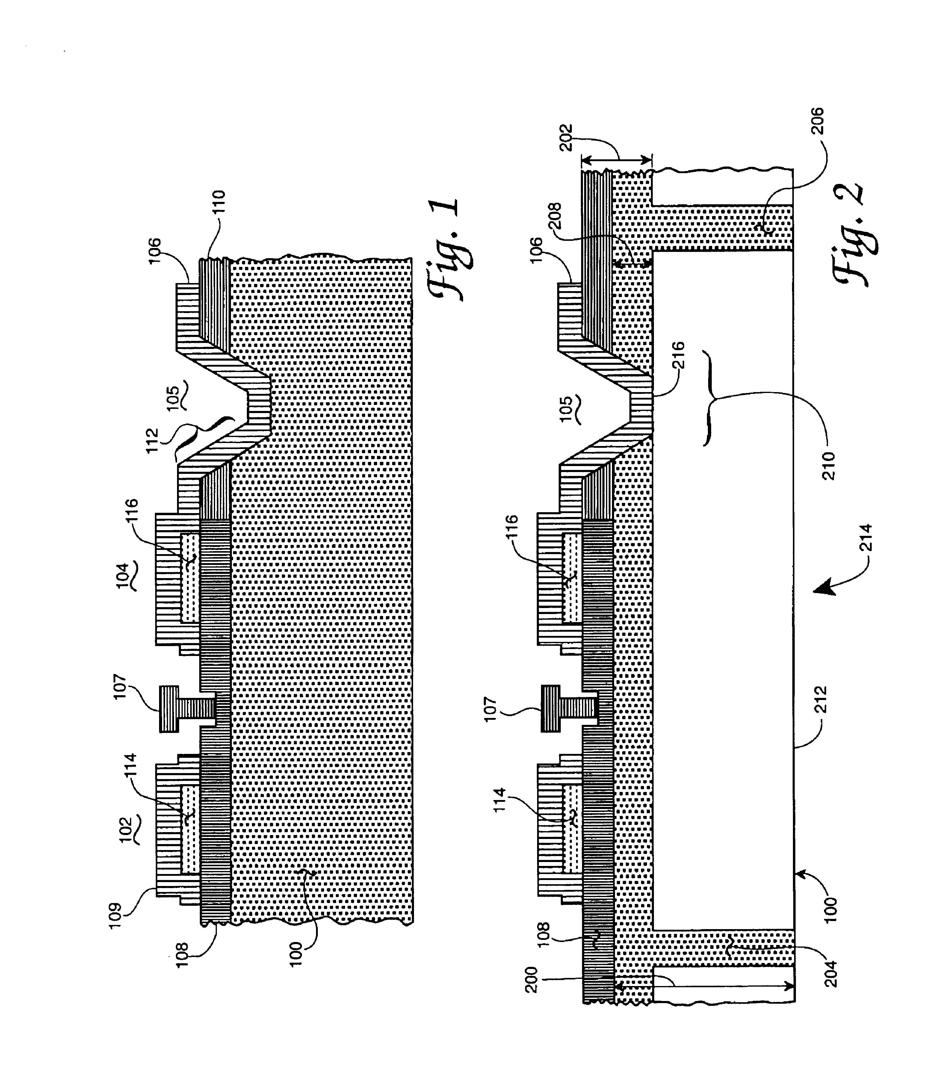
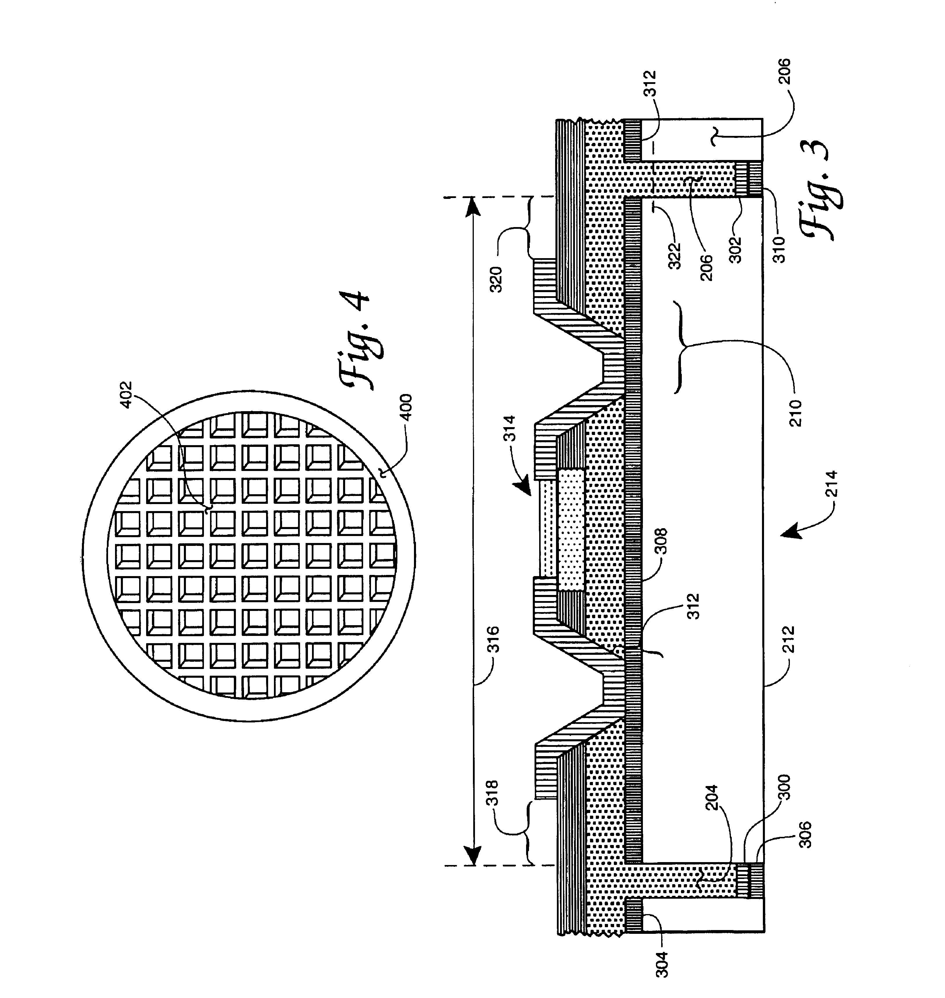
[0027]FIG. 1 in the drawings shows a profile view of a field effect transistor of a type that may be employed in a radio frequency integrated circuit device. The FIG. 1 transistor is shown in a not to scale cross sectional view representing the state of the transistor following completion of the transistor fabrication sequence and representing partial accomplishment of the complete wafer multiple transistor fabrication process i.e., following completion of the wafer frontal side processing but prior to commencement of the wafer backside processing. In this state of completion several aspects of the present wafer backside invention may be conveniently viewed and discussed. The FIG. 1 transistor may be considered to be of gallium arsenide composition although transistors made of silicon and other materials are equally viable as hosts for the present invention. In FIG. 1 it is notable that via holes are normally formed on the backside of a wafer, after wafer thinning, and while the waf...


PUM


Abstract

An etching based semiconductor wafer thinning arrangement usable as an improved alternative to the usual grinding and polishing wafer thinning. The thinned wafer includes a structurally enhancing wafer backside grid array of original wafer thickness semiconductor material with grid cells surrounding individual thinned wafer areas and serving to improve the strength and physical rigidity characteristics of the thinned wafer. Preferably this grid array is supplemented with an additional, wafer periphery-located, backside ring of semiconductor material also of original wafer thickness. Ability to avoid a wafer front side mounting during thinning accomplishment, fast etching, reduced wafer breakage, enhanced wafer strength and improved wafer handling achieved with the disclosed thinning arrangement all contribute to achieved advantages over conventional wafer thinning. Gallium arsenide or other semiconductor materials are contemplated along with use in radio frequency or other integrated circuit devices of either the single transistor or complete integrated circuit components types.

Description

CROSS REFERENCE TO RELATED PATENT DOCUMENTS[0001]The present document is somewhat related to the copending and commonly assigned patent application document “MEASURED VIA HOLE ETCHING”, Ser. No. 10 / 034,747 filed of even date herewith. The contents of this related, even filing date application, are hereby incorporated by reference herein.RIGHTS OF THE GOVERNMENT[0002]The invention described herein may be manufactured and used by or for the Government of the United States for all governmental purposes without the payment of any royalty.BACKGROUND OF THE INVENTION[0003]Semiconductor wafers are normally cut at least 500 μm to 625 μm in thickness because this is considered the minimum thickness necessary to provide structural integrity during integrated circuit wafer processing. Thinner wafers usually break during processing, at which point processing of the wafer usually stops because it is not cost effective to process wafer pieces of irregular shape in a production line. For microwave...

Claims


Application Information

Patent Timeline
Patent Type & Authority Patents(United States)
IPC IPC(8): H01L21/02H01L21/44H01L21/306H01L21/308H01L21/768H01L21/78H01L23/66
CPCH01L21/306H01L21/3083H01L21/78H01L23/66H01L23/4824H01L21/76898H01L2924/0002H01L2924/00
Inventor DESALVO, GREGORY C.QUACH, TONY K.EBEL, JOHN L.WALKER, ANDERS P.CASSITY, PAUL D.
Owner SANDVIK AB
Why Eureka
Try Eureka