System to identify a wafer manufacturing problem and method therefor

a technology of manufacturing problem and identification system, which is applied in the direction of instruments, semiconductor/solid-state device testing/measurement, nuclear elements, etc., can solve the problems of unappeasible business (as well as individuals) for better, faster and more reliable electronic goods, and the use of semiconductor technology

Inactive Publication Date: 2005-04-26
APPLIED MATERIALS INC
View PDF14 Cites 55 Cited by
  • Summary
  • Abstract
  • Description
  • Claims
  • Application Information

AI Technical Summary

Benefits of technology

[0020]In particular, attributes of defective wafers are used to generate a wafer signature. The signature is then automatically matched with / compared to a number of previously stored wafer map signatures to determine a number of similarity confidence metrics. Preferably, the signature map matching of a particular case is performed in conjunction with a number of other defect attribute matching processes of that case with previously stored cases. If the matching process yields an acceptable similarity metric, the previously stored cases, including aspects such as a wafer map signature is retrieved from the database. Cases are retrieved where a previous problem and associated root cause has been determined. Preferably, the number of cases retrieved is dependent upon a grading applied to the attributes (such as signature) being matched. A determination can then be made as to whether the current case is exhibiting similar defect characteristics to the previously stored case. If a previous root cause has been determined for a similar defect case, an Operator may then inform the wafer manufacturing process of the identified defect. In this manner, early correction of the wafer manufacturing process can be made. Alternatively, if no previous root cause has been determined, the grading of the matching process assists in a further investigation to determine a root cause.

Problems solved by technology

In particular, the increased use of semiconductor technology has resulted from an unappeasable need by business (as well as individuals) for better, smaller, faster and more reliable electronic goods.
This is much more preferable than completing the manufacture of a whole batch of wafers, only to find that a fault existed in the wafer manufacturing process, thereby creating a number of defective wafers or by failure of the wafer during use.
This human visual inspection process is renowned for being inaccurate due to various factors including stress, eye fatigue and boredom of the Operator.
Furthermore, it is prone to human judgment and therefore prone to the inconsistencies due to different perceptions by different Operators as to the significance of a finding.
In addition, the above inspection approach has the disadvantage that the process is very time consuming.
In this regard, there is a lengthy delay before a particular wafer-manufacturing problem is identified, and steps taken to rectify it.
Finally, the human visual inspection process is limited to a set of pre-defined classifications, which may well not encompass the wafer manufacturing problem that resulted in the wafer defect type encountered.

Method used


Image

  • System to identify a wafer manufacturing problem and method therefor
  • System to identify a wafer manufacturing problem and method therefor
  • System to identify a wafer manufacturing problem and method therefor

Examples


Embodiment Construction

[0026]In the context of the following description, the term ‘wafer’ is used to encompass bare wafers, patterned wafers, sawn wafers, whole wafers, etc.

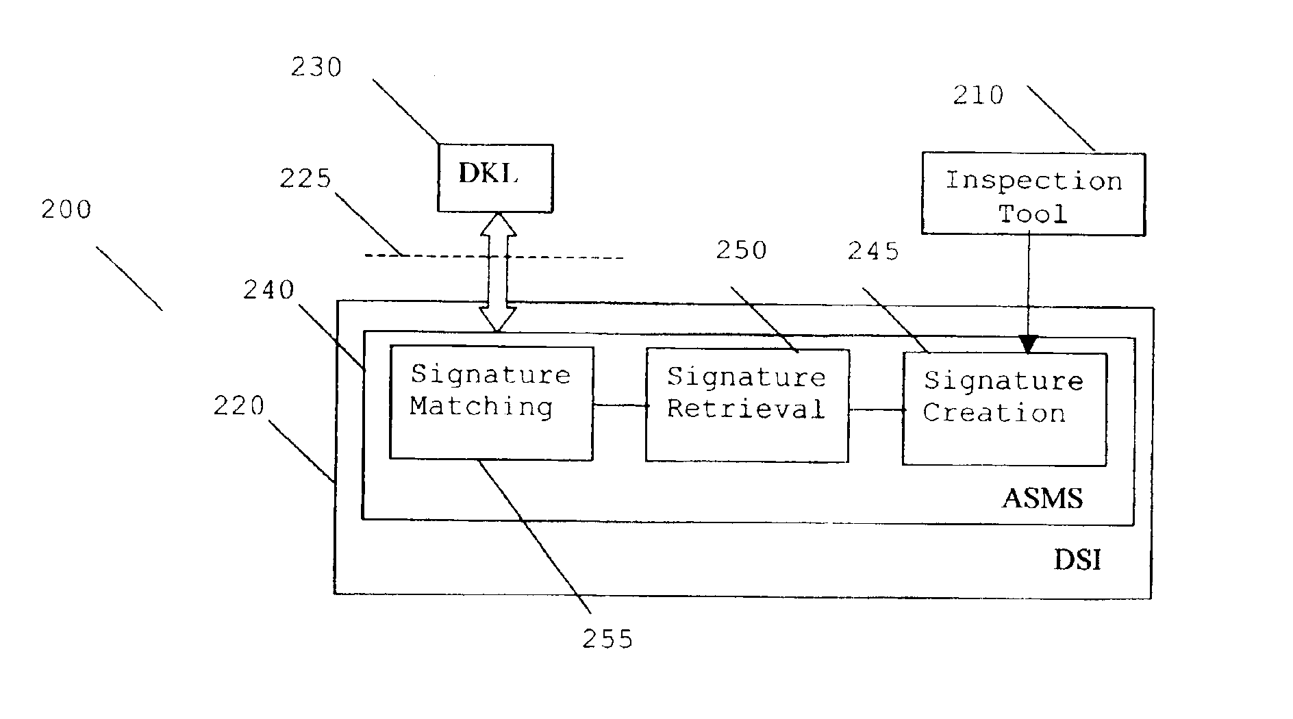
[0027]In summary, the preferred embodiment of the present invention describes an index-based signature retrieval mechanism. The mechanism is preferably implemented by adapting the DSI system, to index and retrieve signatures from a database, such as a DKL, based on their wafer map patterns. The DSI system is further configured to automatically perform the signature matching operation and grade the results to enable a more intelligent and more accurate assessment of the wafer defect similarities. This is a new and unique application for DSI, which has so far been used solely for manual wafer classification. The improved DSI system is used in order to match new wafer signature maps to signature maps previously stored in the DKL database that are known or have been determined as emanating from a particular wafer manufacturing problem.

[00...


PUM


Abstract

A method (400) for determining a response to a wafer manufacturing process problem includes the steps of generating a wafer map signature (406) containing defect attributes to be identified and retrieving (410) one or more wafer map signatures from a database. The wafer map signature to be identified is matched (414) with the one or more wafer map signatures from the database in order to help find a root cause of a defect in a wafer manufacturing process.This provides at least the advantage that a signature matching capability allows an Operator to more accurately identify a root manufacturing cause of a wafer defect. Furthermore, instant feedback to the wafer manufacturing process can be provided to facilitate rapid correction of manufacturing errors.

Description

FIELD OF THE INVENTION[0001]This invention relates to methods and apparatus for determining and identifying a response to a wafer manufacturing process problem. The invention is applicable to, but not limited to, automated signature matching of semiconductor wafers to determine defect types in a manufactured wafer.BACKGROUND OF THE INVENTION[0002]The use of semiconductor technology has, over the last few decades, revolutionized the use of electrical and electronic goods. In particular, the increased use of semiconductor technology has resulted from an unappeasable need by business (as well as individuals) for better, smaller, faster and more reliable electronic goods.[0003]The semiconductor wafer manufacturers have therefore needed to make commensurate improvements in product quality, as well as in the speed, quality and reliability of the semiconductor wafer manufacturing process. Clearly, in the mass-manufacture of semiconductor wafers, the manufacturer needs to minimize the numbe...

Claims


Application Information

Patent Timeline
Patent Type & Authority Patents(United States)
IPC IPC(8): G06F17/30H01L21/66
CPCH01L22/20G06F16/00
Inventor GAVRA, YIFAHDOR, AMOS
Owner APPLIED MATERIALS INC
Why Eureka
Try Eureka