Nonvolatile semiconductor memory device, manufacturing method thereof, and operating method thereof

a semiconductor memory and nonvolatile technology, applied in semiconductor devices, electrical devices, instruments, etc., can solve the problems of reducing the size and/or operation voltage, affecting the holding characteristic of information charges, and affecting the operation speed. , to achieve the effect of high melting point polycide films

Inactive Publication Date: 2005-05-03
RENESAS ELECTRONICS CORP
View PDF4 Cites 132 Cited by
  • Summary
  • Abstract
  • Description
  • Claims
  • Application Information

AI Technical Summary

Benefits of technology

[0046]According to one aspect of the embodiments, the present invention may also include a first conductive film being a polycrystalline silicon film containing an impurity and a second conductive film having a high melting point polycide film.

Problems solved by technology

However, current mass produced flash memory products appear to use only FG type transistors as the nonvolatile memory element.
However, such reductions in size and / or operation voltage can work against the goal of increasing operating speed.
In a FG gate type transistor, a holding characteristic for the information charge can suffer if an insulating film surrounding a floating gate is not sufficiently thick.
However, such a tunneling oxide thickness can require a certain operating erasure potential to ensure adequate charge transfer in a write or erase operation.
In addition, the manufacturing processes for FG type flash memory products can be complex and hence difficult to simplify.
Because of this, it can be difficult to reduce the cost of manufacturing such flash memory products.
Such a minimum thickness can result in drawbacks.
Limits in minimum thickness of an insulating film (or films) can result corresponding limits in the read speed of such devices.
This can reduce the effective channel length of the resulting transistor device.
Such an arrangement can be difficult to achieve with the second conventional example.
Such small widths can present an increased wiring resistance that introduces delay into signal transmission.
In view of this, it can be difficult to incorporate such an approach into memory cell array applications.

Method used


Image

  • Nonvolatile semiconductor memory device, manufacturing method thereof, and operating method thereof
  • Nonvolatile semiconductor memory device, manufacturing method thereof, and operating method thereof
  • Nonvolatile semiconductor memory device, manufacturing method thereof, and operating method thereof

Examples


Embodiment Construction

[0077]The present invention will hereinafter be described in more detail on the basis of various particular embodiments with reference to accompanying figures.

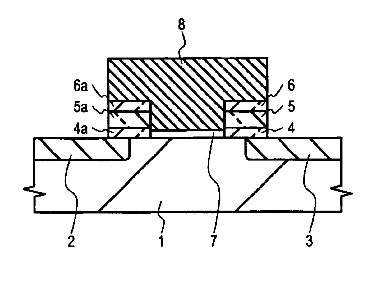
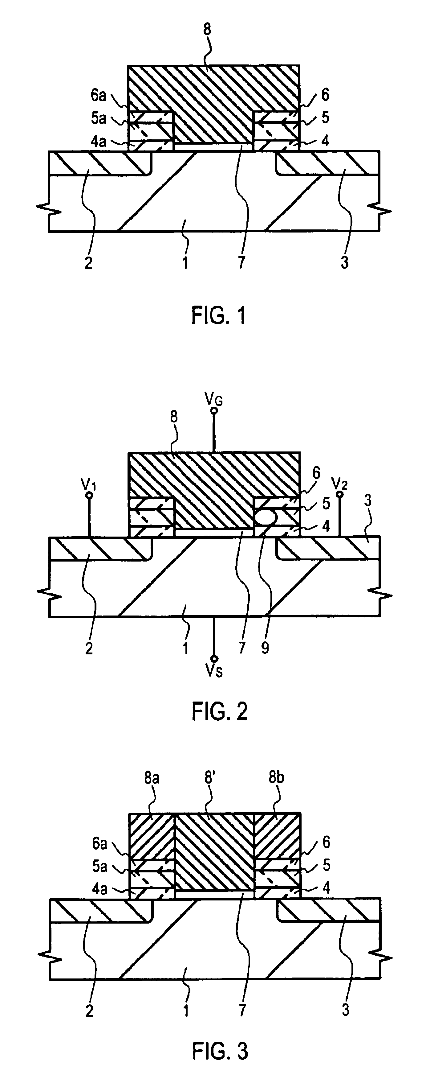
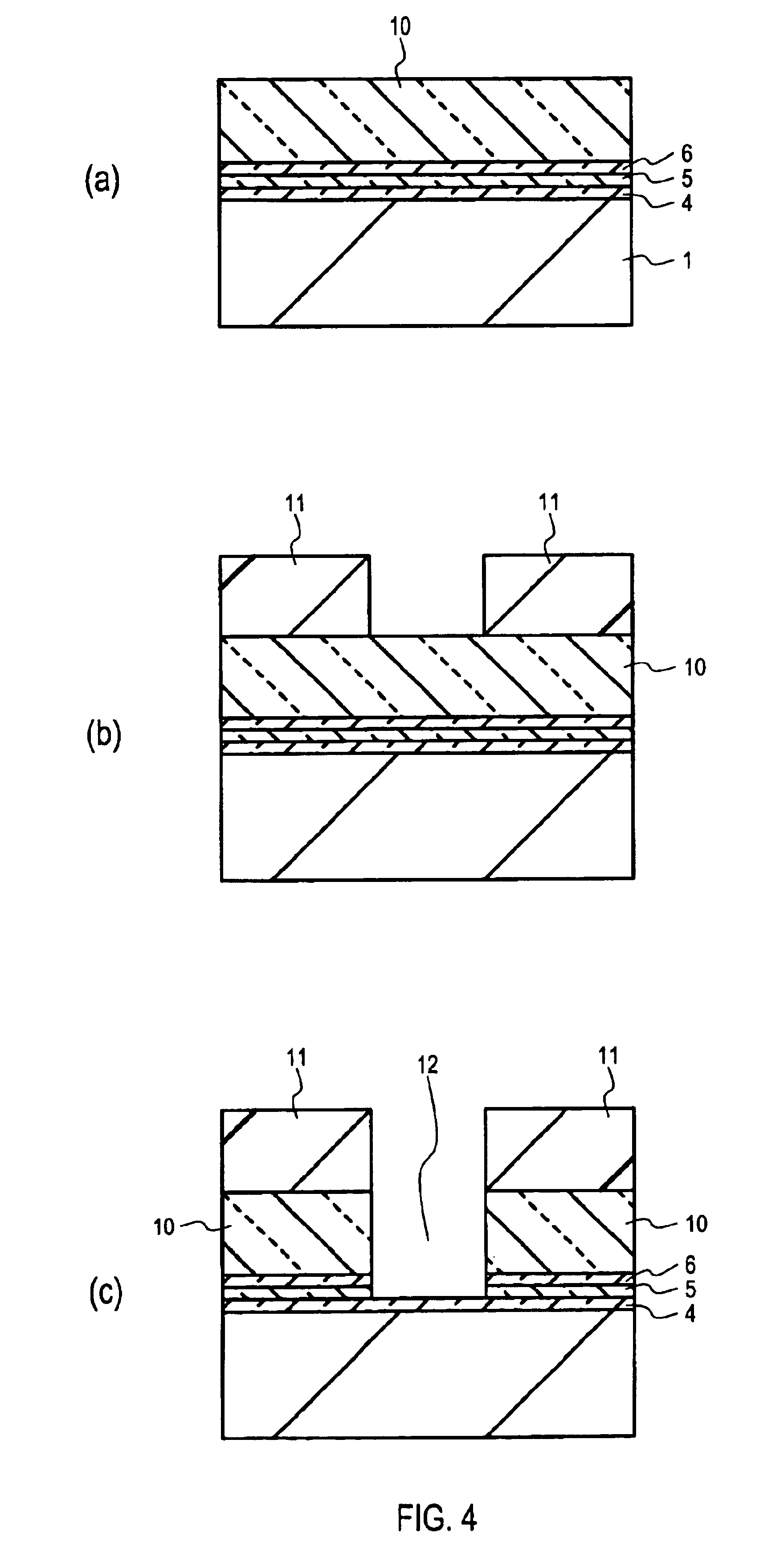
[0078]Embodiments of the present invention will now be described with reference to FIGS. 1 to 9(c). FIGS. 1 and 3 are sectional views showing the basic structure of a nonvolatile memory element according to the present invention, which may be used in a flash memory. FIGS. 4(a) to 9(c) are sectional views showing various steps according to a manufacturing method according to an embodiment.

[0079]Referring to FIG. 1, a nonvolatile memory element may include a first diffusion layer 2, a second diffusion layer 3, and a substrate 1. A substrate 1 may include silicon, more particularly silicon of a P-conductivity type. First and second diffusion layers (2 and 3) may include N+ diffusion layers in the substrate 1. A nonvolatile memory element may further include a laminate film near a first diffusion layer 2 and / or a second diffusion ...


PUM


Abstract

Nonvolatile memory elements are disclosed which can have increased capacity, reduced operating voltage and/or faster operating speeds. According to one embodiment, a nonvolatile memory element can include a first diffusion layer (2) and a second diffusion layer (3) formed in a main surface of a substrate (1). A laminate film can be formed near a first diffusion layer (2) and/or a second diffusion layers (3) that includes a first insulating film (4a or 4), a second insulating film (5a or 5), and a third insulating film (6a or 6). A gate insulating film (7) can be formed a channel region and gate electrode (8) can be formed to cover gate insulating film (7) and the laminate film(s) that has a T-shape. A gate electrode (8) can have end portions that sandwich a first insulating film (4a or 4), a second insulating film (5a or 5), and a third insulating film (6a or 6) with a first diffusion layer (2) and/or second diffusion layer (3).

Description

TECHNICAL FIELD[0001]The present invention relates generally to a nonvolatile semiconductor memory device, manufacturing method and operating method, and more particularly to a Metal Oxide Nitride Oxide Semiconductor (MONOS) type nonvolatile memory device, manufacturing method and operating method.BACKGROUND OF THE INVENTION[0002]In general, nonvolatile memory devices of the metal-insulator-semiconductor (MIS) type can be broadly divided into two basic types of devices: Metal Nitride Oxide Semiconductor (MNOS) type transistors and floating gate (FG) type transistors.[0003]MNOS type transistors typically store a charge, which can represent information, within one or more insulating films of a gate insulating film. For example, in the case of a two-layer gate insulating film, charge may be stored at interface states, or the like, formed at a boundary layer between two insulating films. One example of such an arrangement can be an MNOS type device. In addition to such a two-layer arran...

Claims


Application Information

Patent Timeline
Patent Type & Authority Patents(United States)
IPC IPC(8): H01L21/02H01L27/115H01L21/70H01L21/28H01L29/66H01L21/8246H01L29/792G11C16/04H01L21/8247H01L29/788
CPCH01L21/28282H01L29/7923H01L27/11568H01L27/115G11C16/0475H01L29/40117H10B43/30H10B69/00
Inventor YOSHINO, AKIRA
Owner RENESAS ELECTRONICS CORP
Why Eureka
Try Eureka