Systems for buried electrical feedthroughs in a glass-silicon MEMS process

Inactive Publication Date: 2005-05-03
HONEYWELL INT INC
View PDF25 Cites 30 Cited by
  • Summary
  • Abstract
  • Description
  • Claims
  • Application Information

AI Technical Summary

Problems solved by technology

Unfortunately, using this method it is difficult to make a silicon structure, for example, a vibrating sensor, that is completely enclosed by the cavity but not connected to the cavity walls.
A seal is much more difficult to attain since formation of the electrical leads form uneven topography on the glass substrate surface.
The gaps result in an uneven sealing surface and result in unbonded areas which break the hermetic seal.
However, anodic bonding can only be accomplished over uneven areas that fluctuate by about 200 angstroms or less, and a long term leak rate for anodic bonding seals is unknown.

Method used


Image

  • Systems for buried electrical feedthroughs in a glass-silicon MEMS process
  • Systems for buried electrical feedthroughs in a glass-silicon MEMS process
  • Systems for buried electrical feedthroughs in a glass-silicon MEMS process

Examples


Embodiment Construction

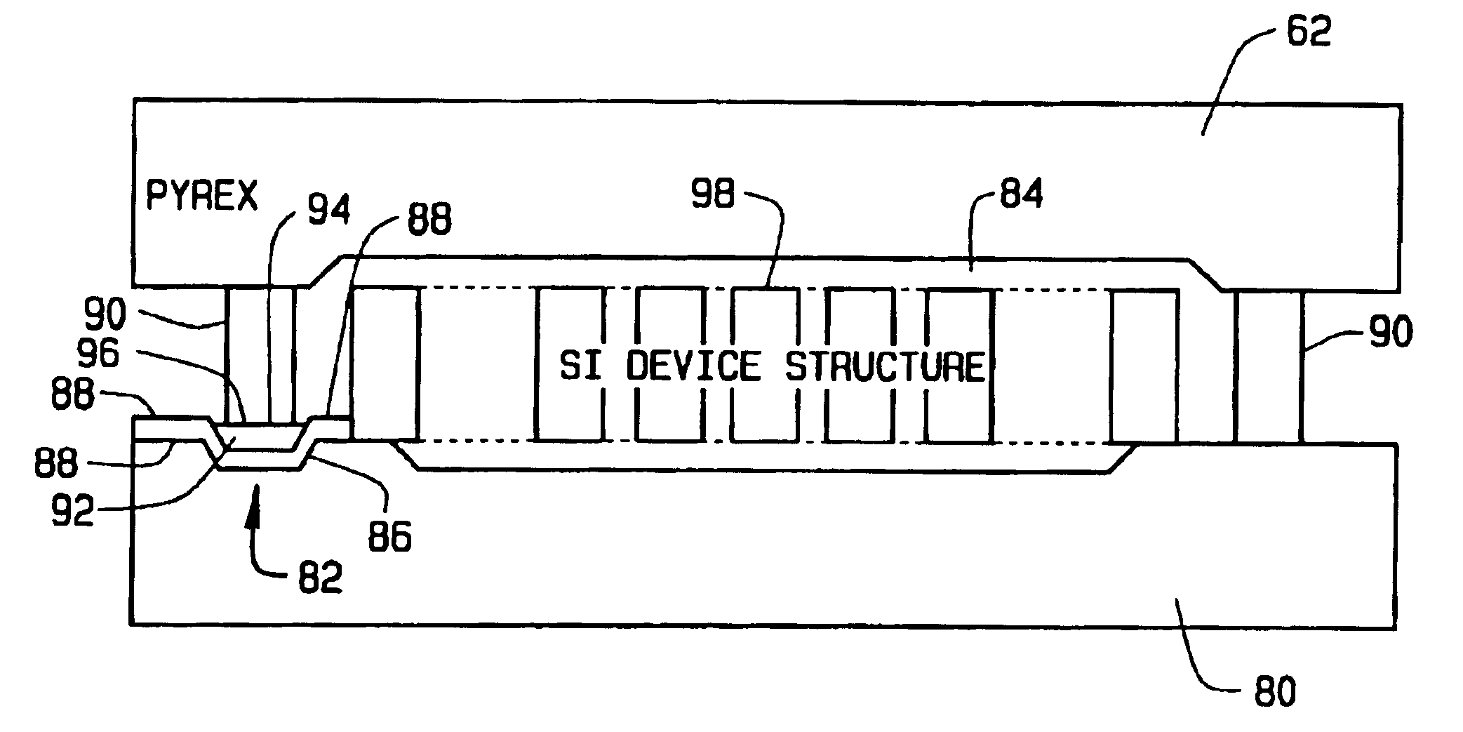
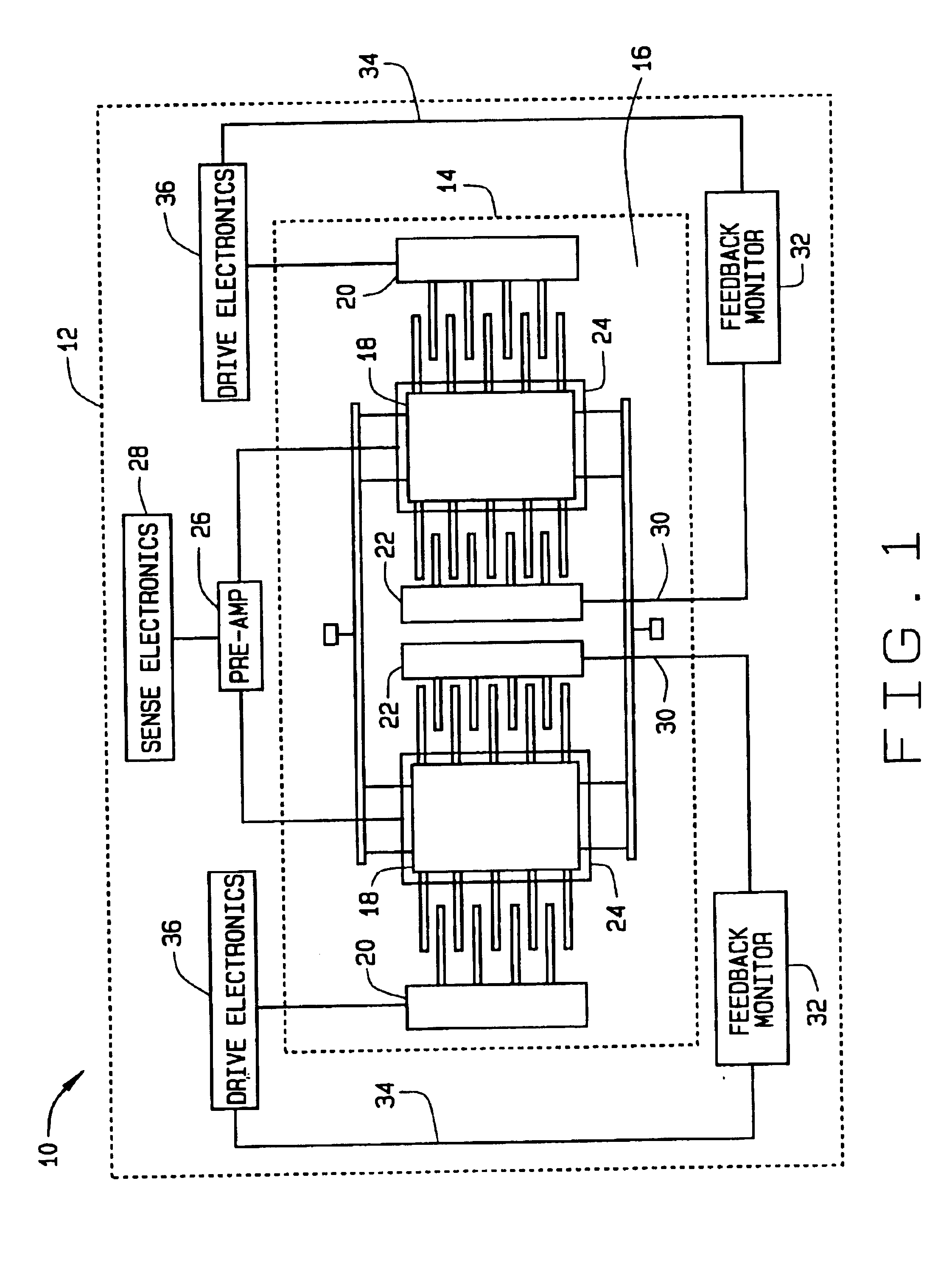
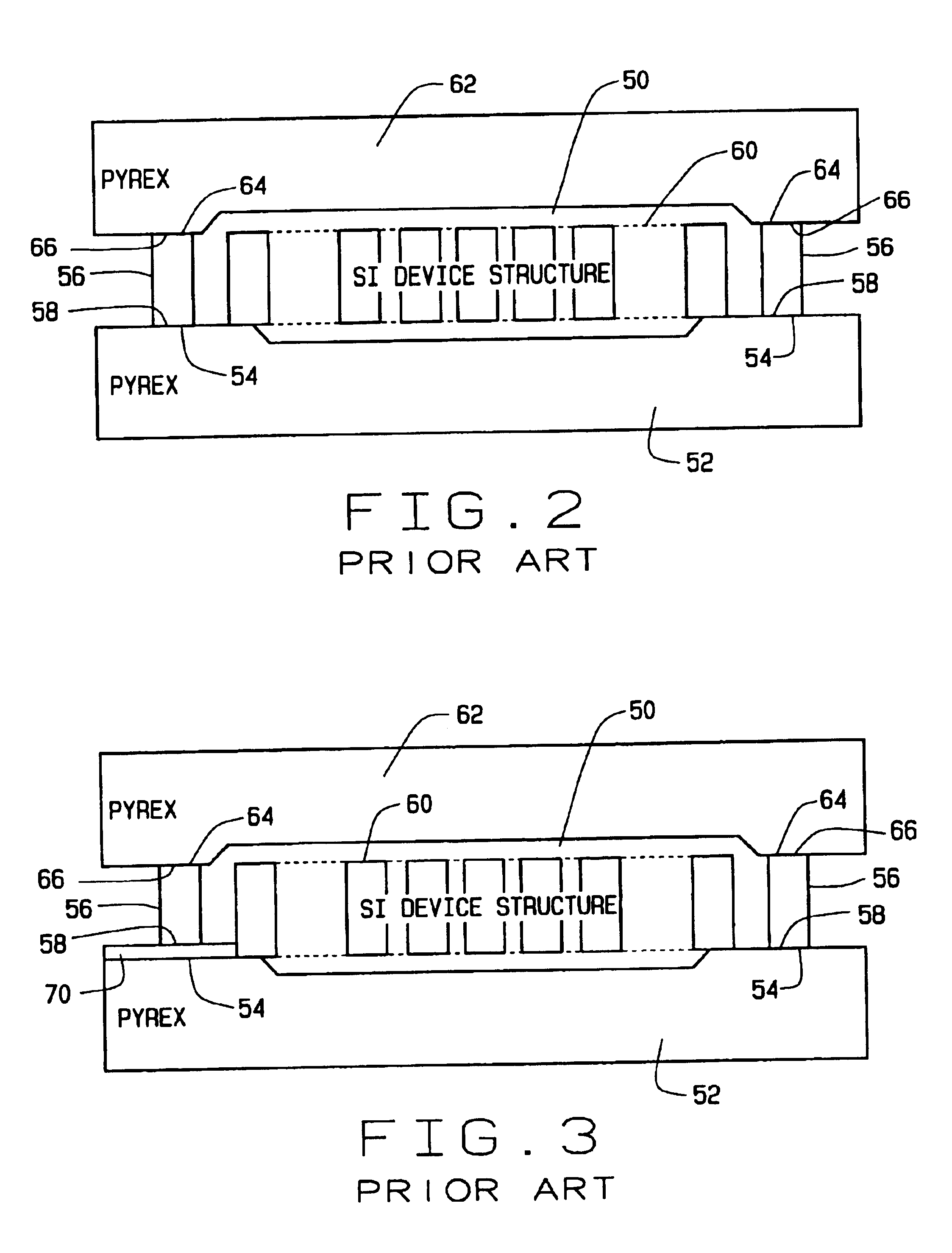
[0022]FIG. 1 is a schematic illustration of a micro electromechanical system (MEMS) gyroscope 10. MEMS gyroscope 10 may include a housing 12 that includes therein a tuning fork gyroscope (TFG) 14. Housing 12 may be a plastic package, a small outline integrated circuit (SOIC) package, a plastic leadless chip carrier (LCC) package, a quad flat package (QFP), or other housings as known in the art. Housing 12 may provide a structure to co-locate elements of TFG 14 and / or locate other elements within a close proximity of one another within the housing 12. TFG 14, in one embodiment, is located within a substantially sealed cavity 16 which is formed by bonding silicon to a glass substrate. Substantially sealed cavity 16 provides separation between sensitive elements of TFG 14 and drive electronics, described below.

[0023]In one embodiment, TFG 14 may include proof masses 18, motor drive combs 20, motor pickoff combs 22, and sense plates 24. A pre-amplifier 26 may be included within housing ...


PUM


Abstract

A method for providing conductive paths into a hermetically sealed cavity is described. The sealed cavity is formed utilizing a silicon-glass micro-electromechanical structure (MEMS) process and the method includes forming recesses on a glass substrate everywhere that a conductive path is to pass into the cavity, and forming conductive leads in and around the recesses. A glass layer is deposited over the substrate, into the recesses, and over the conductive leads and then planarized to expose portions of the conductive leads. A sealing surface is formed on at least a portion of the glass layer. Silicon is then bonded to the sealing surface of the planarized glass layer, the wafer being configured such that a portion of each lead is within the sealed cavity and a portion of each lead is outside the sealed cavity.

Description

BACKGROUND OF THE INVENTION[0001]This invention relates generally to micro-electromechanical structures (MEMS) processes, and more specifically to electrical connections from the inside to the outside of a sealed cavity formed in MEMS processes.[0002]One method of producing micro-electromechanical structures (MEMS) is by bonding a patterned silicon wafer to a glass (usually pyrex) substrate. Portions of the silicon wafer are etched away, leaving a mechanical silicon structure anchored to the glass substrate. The process is initiated with a glass wafer. A cavity is formed in the wafer using a wet or dry etching process. A depth of the etch determines a separation between the structure's capacitive elements. Metal layers are deposited and patterned on the glass, forming conductive electrodes and interconnects. A heavily boron doped (p++) epitaxial layer is grown on a separate, lightly doped silicon substrate. A pattern is etched into the silicon wafer to a depth greater than the thick...

Claims


Application Information

Patent Timeline
IPC IPC(8): B81B7/00
CPCB81C1/00301B81B2207/097B81C1/00G01P15/08B81B7/02B81B7/00
Inventor HORNING, ROBERT D.RIDLEY, JEFFREY A.
Owner HONEYWELL INT INC
Why Eureka
Try Eureka