Nonvolatile memory device

a memory device and non-volatile technology, applied in semiconductor devices, digital storage, instruments, etc., can solve the problems of difficult to accurately control the state at 3-level or larger multi-level storage in variable resistor elements, complex cell structure, and high integration, so as to improve multi-level storage capacity and improve read operation. , the effect of high speed

Active Publication Date: 2005-05-03
XENOGENIC DEV LLC
View PDF3 Cites 68 Cited by
  • Summary
  • Abstract
  • Description
  • Claims
  • Application Information

AI Technical Summary

Benefits of technology

[0017]According to the feature configuration described above, the difference in the resistance values corresponding to two or more program states can be set to be large, so that high speed and steady read operation can be imple

Problems solved by technology

However, since the nonvolatile memory devices have a structure in which electrical charges are accumulated in the floating gates with high electric fields, the cell structure is complex to an extent of giving rise to problems in implementing high integration.
However, OUM memories according to conventional techniques use principles of storing the data in the manner that the memory layer is electrically controlled to change between the two states, i.e., crystalline and noncrystalline states, and therefore give problems of making it difficult to accurately control the states at 3-level or larger multi-level to be stored in variable resistor elements formed of a single property material.
However, the memory element gives to a problem of increasing manufacturing steps.
In addition, there arises another problem in that, when the number of program levels is

Method used


Image

  • Nonvolatile memory device
  • Nonvolatile memory device
  • Nonvolatile memory device

Examples


Embodiment Construction

[0040]An embodiment of a nonvolatile memory device (which hereinbelow will be alternatively referred to as a “present inventive device” in appropriate portions) according to the present invention will be described hereinbelow with reference to the accompanying drawings.

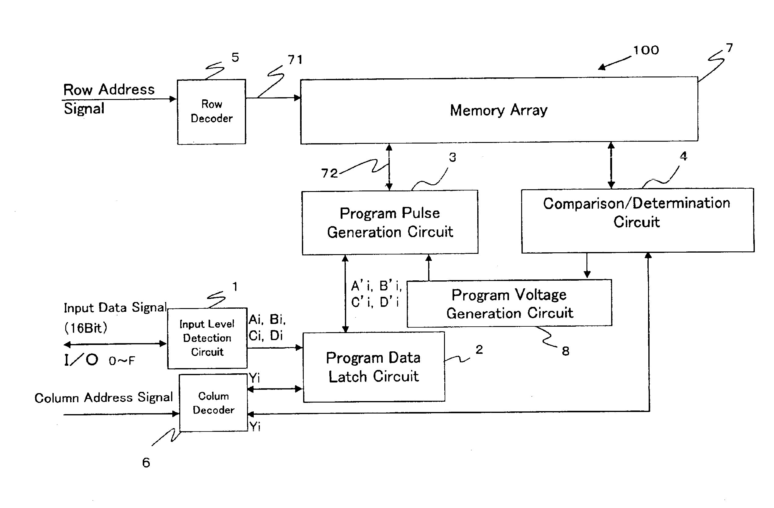
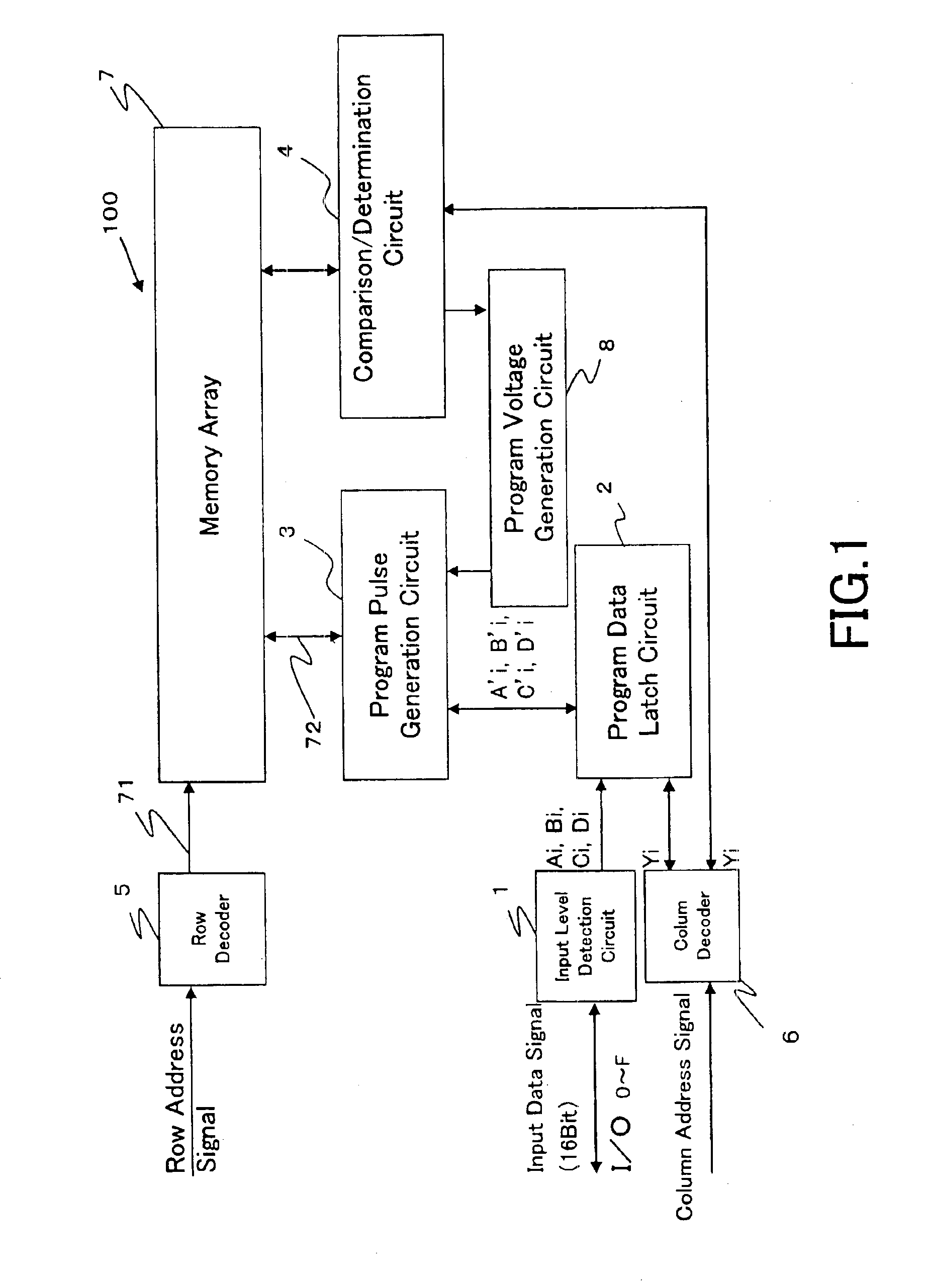
[0041]FIG. 1 is a functional block configuration diagram of a present inventive device 100. The present inventive device 100 has a function of storing externally input 16 bits of 2-level data in eight memory cells. Each of the memory cells is capable of storing 4-level data (2 bits).

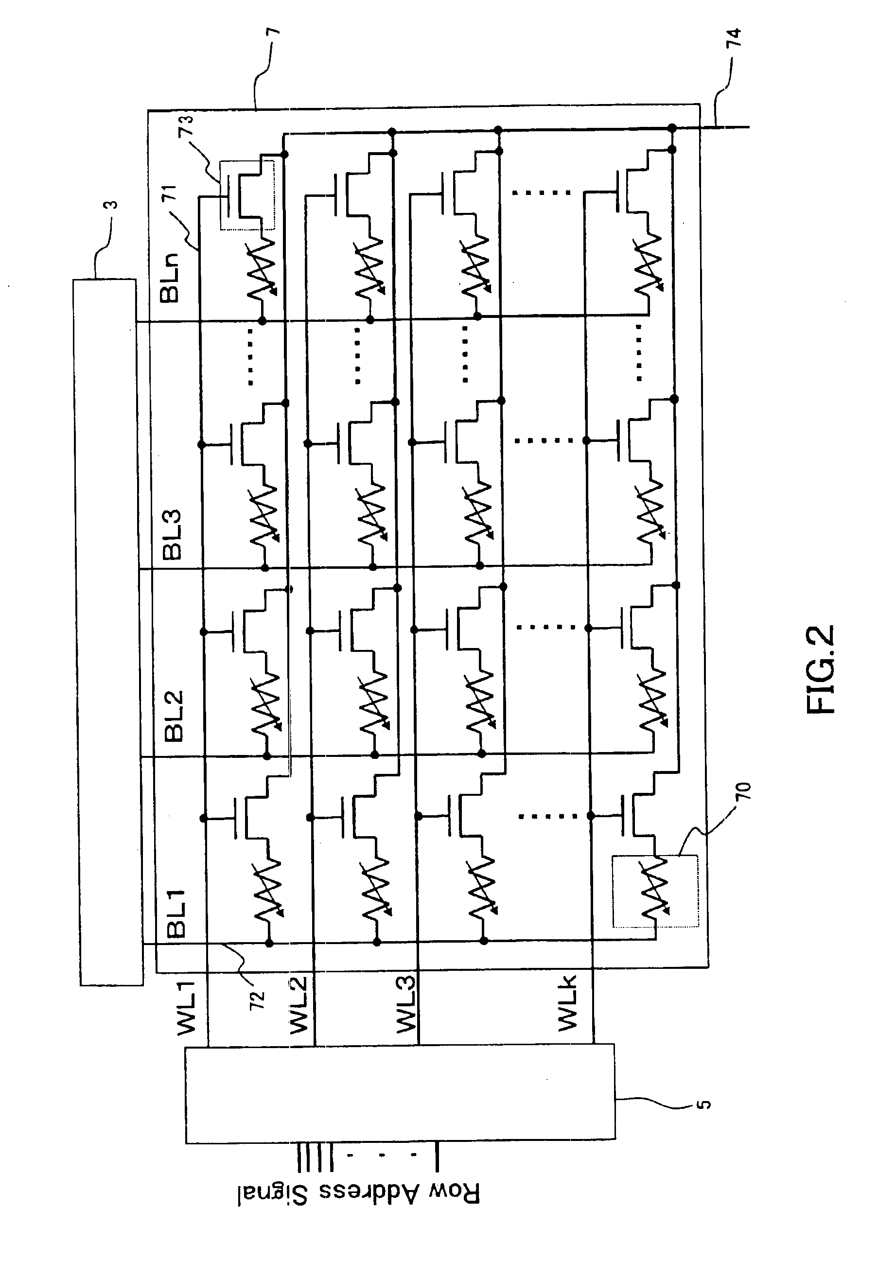
[0042]The present inventive device 100 has an input level detection circuit 1, a program data latch circuit 2, a program pulse generation circuit 3, a comparison / determination circuit 4, a row decoder 5, a column decoder 6, a memory array 7, and a program voltage generation circuit 8. In addition, although not shown in the drawing, the present inventive device has a control circuit for controlling the entirety of functional blocks, and a r...


PUM


Abstract

An object of the present invention is to provide a mass-storage nonvolatile memory device capable of performing high speed operation. The nonvolatile memory device comprises a memory array comprising a plurality of memory cells arranged in a matrix, each of the memory cells comprising a variable resistor element formed of a manganese-containing oxide having a perovskite structure in which an electric resistance is varied by application of a voltage pulse and a variation amount of the electric resistance is variable depending on the magnitude of the voltage amplitude; and a program pulse generation circuit that, in order to program 3-level or larger multi-level data corresponding to one erase state and two or more program states into the variable resistor element, is capable of performing generation of program pulses having two or more different voltage amplitudes corresponding to the program states, the generation being separately performed corresponding to program data.

Description

BACKGROUND OF THE INVENTION[0001]1. Field of the Invention[0002]The present invention relates to nonvolatile memory devices; and more specifically, the invention relates to a nonvolatile memory device that, using variable resistor elements permitting an electric resistance to be variable for each memory cell, is capable of storing. 2-level, 3-level, or a larger multi-level data into one memory cell by utilizing variations in the electric resistance.[0003]2. Description of the Related Art[0004]Nonvolatile memory devices are widely used by being mounted in various mobile apparatuses, such as cellular phones, IC cards, and digital cameras. In recent years, in line with increasing opportunities of handling image data, demands have been growing for nonvolatile memories capable of storing even larger amount of data and operating at higher speed. In addition, since such nonvolatile memory devices are intended for use with mobile apparatuses, demands for low power consumption are even more ...

Claims


Application Information

Patent Timeline
IPC IPC(8): G11C11/56G11C16/02G11C13/00G11C11/15H01L27/10H01L27/105H01L45/00
CPCG11C11/5685G11C13/0007G11C2213/79G11C2213/31G11C11/15
Inventor EHIRO, MASAYUKIINOUE, KOJIAWAYA, NOBUYOSHI
Owner XENOGENIC DEV LLC
Why Eureka
Try Eureka