Semiconductor integrated device

Inactive Publication Date: 2005-05-03
LAPIS SEMICON CO LTD
View PDF4 Cites 8 Cited by
  • Summary
  • Abstract
  • Description
  • Claims
  • Application Information

AI Technical Summary

Benefits of technology

[0007]In view of the above problems, an object of the present invention is to

Problems solved by technology

There is also the problem that the output section operates increasing con

Method used


Image

  • Semiconductor integrated device
  • Semiconductor integrated device
  • Semiconductor integrated device

Examples


embodiment 1

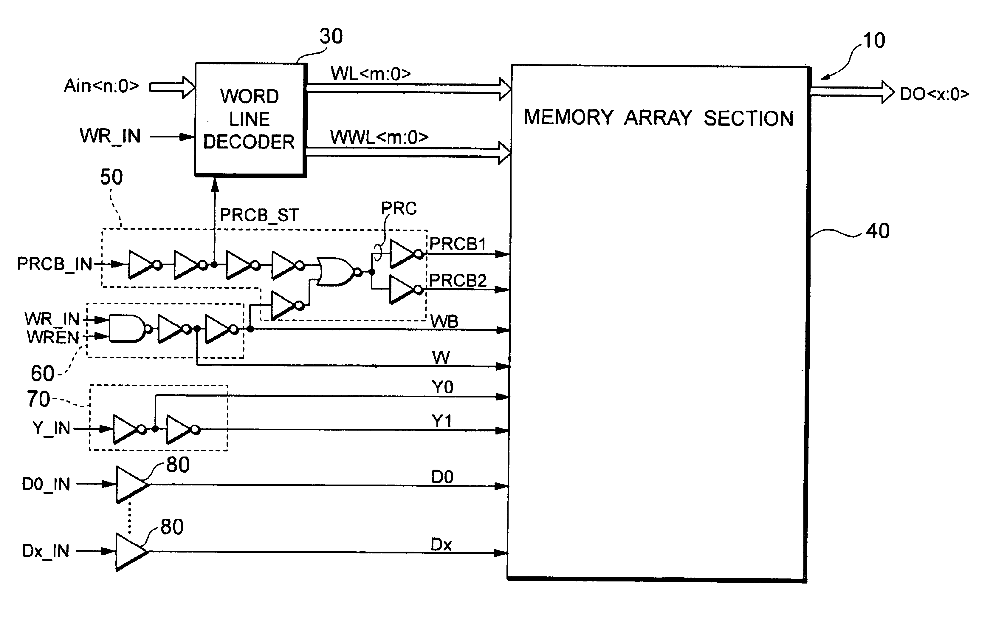
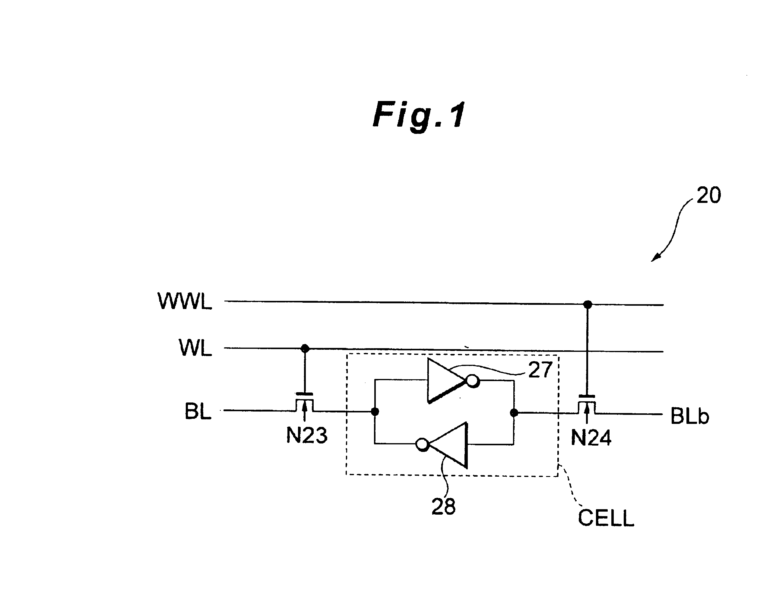
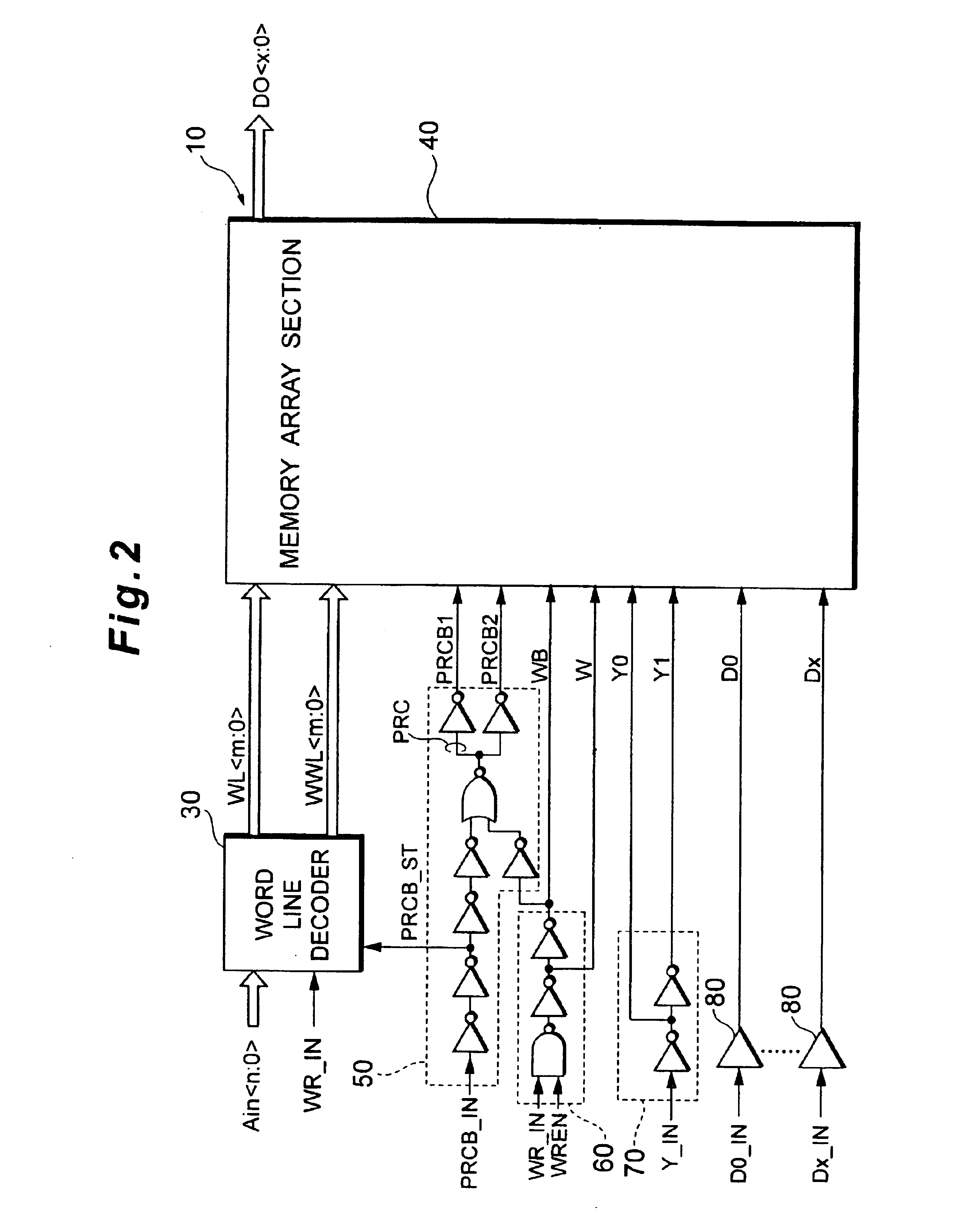
[0103]As described above, according to the semiconductor integrated device 10 of the embodiment 1, the memory cell connected with the BLb is electrically cut off from the BLb by the WL when reading out the bit information indicating the high potential. Thus, the number of times of charge and discharge can be suppressed, and thereby consumption current can be reduced.

[0104]Next, a semiconductor integrated device which comprises the memory array section 110 provided with a cutoff section 112 cutting off signals causing unnecessary operation in the output section 100 will be described.

[0105]The semiconductor integrated device of the embodiment 2 is the same in configuration as the embodiment 1 shown in FIG. 2, but is provided with a cutoff control signal generator 61 as a new part. In the embodiment 1, the memory array section is controlled using the WB generated by the write control signal generator 60, but in the embodiment 2, the memory array section 110 is controlled using a cutoff...

embodiment 2

[0120]According to the semiconductor integrated device of the embodiment 2, by providing the cutoff section 112 preventing the output section 100 from operating needlessly, a signal is supplied to the output section 100 only during the write period for memory cells. Thus, the output section 100 does not operate needlessly, thereby reducing IDD.

[0121]A semiconductor integrated device provided with an equalizer 113 cutting a bit line pair off from a potential supply port for pre-charge and equalizing potentials held in the bit line pair will be described.

[0122]As shown in FIG. 10, the memory array section 120 of embodiment 3 is, in configuration, the memory array section 110 of embodiment 1 provided with the equalizer 113, which operates based on a third pre-charge control signal for controlling pre-charge (hereinafter, simply called PRCB3).

[0123]The equalizer 113 comprises a first PMOS (hereinafter, called P1) that cuts off VDD for pre-charging the BL based on the PRCB3; a second PMO...

embodiment 3

[0134]According to the semiconductor integrated device of the embodiment 3, the equalizer 113 is provided so that during one in two consecutive readouts, the potentials of the BL and BLb are equalized during the pre-charge period to read out bit information with this potential as pre-charge. Thus, consumption current can be reduced.

[0135]A semiconductor integrated device which comprises a memory array section 130 provided with an equalizer 114 having NMOSs cutting off a bit line pair instead of the PMOSs, which cut the bit line pair off from the pre-charge potential supply port in the equalizer 113 of the embodiment 3, will be described.


PUM


Abstract

A semiconductor integrated device which comprises a memory cell 20 holding bit information; a pair of bit lines connected to the memory cell via which the bit information is input and output in predetermined cycles; and an output section 100 that latches an output from the memory cell via one bit line of the pair and the other bit line and outputs the bit information acquired from the one bit line as a result of reading from the memory cell, and which pre-charges the pair of bit lines before access to the memory cell. The memory cell 20 has a cutoff circuit (N24) that cuts off the other bit line to hold voltage thereof produced by pre-charging when the bit information held in the memory cell is read out.

Description

BACKGROUND OF THE INVENTION[0001]1. Field of the Invention[0002]The present invention relates to a semiconductor integrated device, and particularly to a memory device called SRAM (Static Random Access Memory).[0003]2. Description of the Related Art[0004]SRAM as a semiconductor integrated device comprises a plurality of memory cells, and each memory cell is connected to a pair of bit lines. Via the pair of bit lines, bit information indicating whether an electric potential exists is written into the memory cell, and bit information held in the memory cell is read out. Such write and read access to the memory cell is performed after applying a potential called pre-charge to the pair of bit lines. The memory cell can be accessed at high speed by having pre-charged. As mentioned above, after having pre-charged, bit information read out from the memory cell is output via an output section. Such semiconductor devices are disclosed in Japanese Patent Laid-Open Publication No. 11-86561 and...

Claims


Application Information

Patent Timeline
IPC IPC(8): G11C7/12G11C7/00G11C11/41G11C11/418
CPCG11C7/12
Inventor SUGIO, KENICHIRO
Owner LAPIS SEMICON CO LTD
Why Eureka
Try Eureka