Plated probe structure

a probe structure and probe technology, applied in the field of probe structures, can solve the problems of easy deformation or damage of probe wires, high cost of fabricating contemporary probes for testing integrated circuits, and high cost of individual semiconductor device testing, etc., to facilitate the alignment of solder ball connections, facilitate oxide penetration, and reduce the length of electrical conductors

Inactive Publication Date: 2005-05-10
WL GORE & ASSOC INC
View PDF4 Cites 22 Cited by
  • Summary
  • Abstract
  • Description
  • Claims
  • Application Information

AI Technical Summary

Benefits of technology

[0011]Another object of the present invention is to provide a probe structure that is an integral part of the fan out wiring on the test substrate or other printed wiring means to minimize the electrical conductor length as well as the contact resistance of the probe interface.
[0012]A further object of the present invention is to pr...

Problems solved by technology

If the integrated circuit device is defective, the device and the plastic leaded chip carrier are discarded.
The semi-permanent attachment techniques used for testing integrated circuit devices such as solder ball attachment to a ceramic or plastic pin grid array package are typically used for devices that have high number of interconnections and the pin grid array package is relatively expensive.
If the integrated circuit device is defective, the device can be removed from the pin grid array package by heating the solder balls to their melting point.
Contemporary probes for testing integrated circuits are expensive...

Method used


Image

  • Plated probe structure
  • Plated probe structure
  • Plated probe structure

Examples


Embodiment Construction

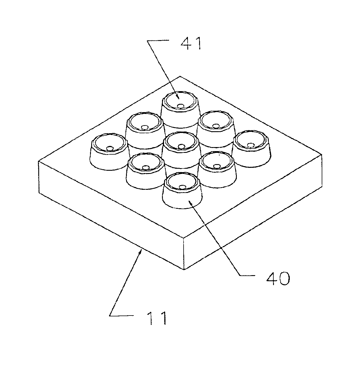
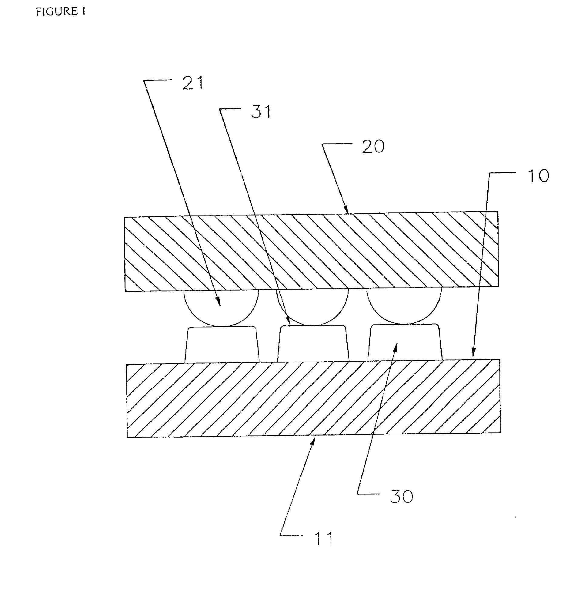
[0036]In a preferred embodiment, FIG. 1 shows a cross section of a test substrate (11) and a plated test probe (30) according to the present invention. The test substrate (11) provides a rigid base for attachment of the probes (30) and fan-out wiring from the high density array of probe contacts to a larger grid of pins or other interconnection means to the equipment used to electrically test the integrated circuit device. The fan out substrate can be made from various materials and constructions including single and multi-layer ceramic with thick or thin film wiring, silicon wafer with thin film wiring or epoxy glass laminate construction with high density copper wiring. Test probes (30) are attached to the first surface (10) of the substrate (11). The probes are used to contact the solder ball connections (21) on the integrated circuit device (20) at surface (31).

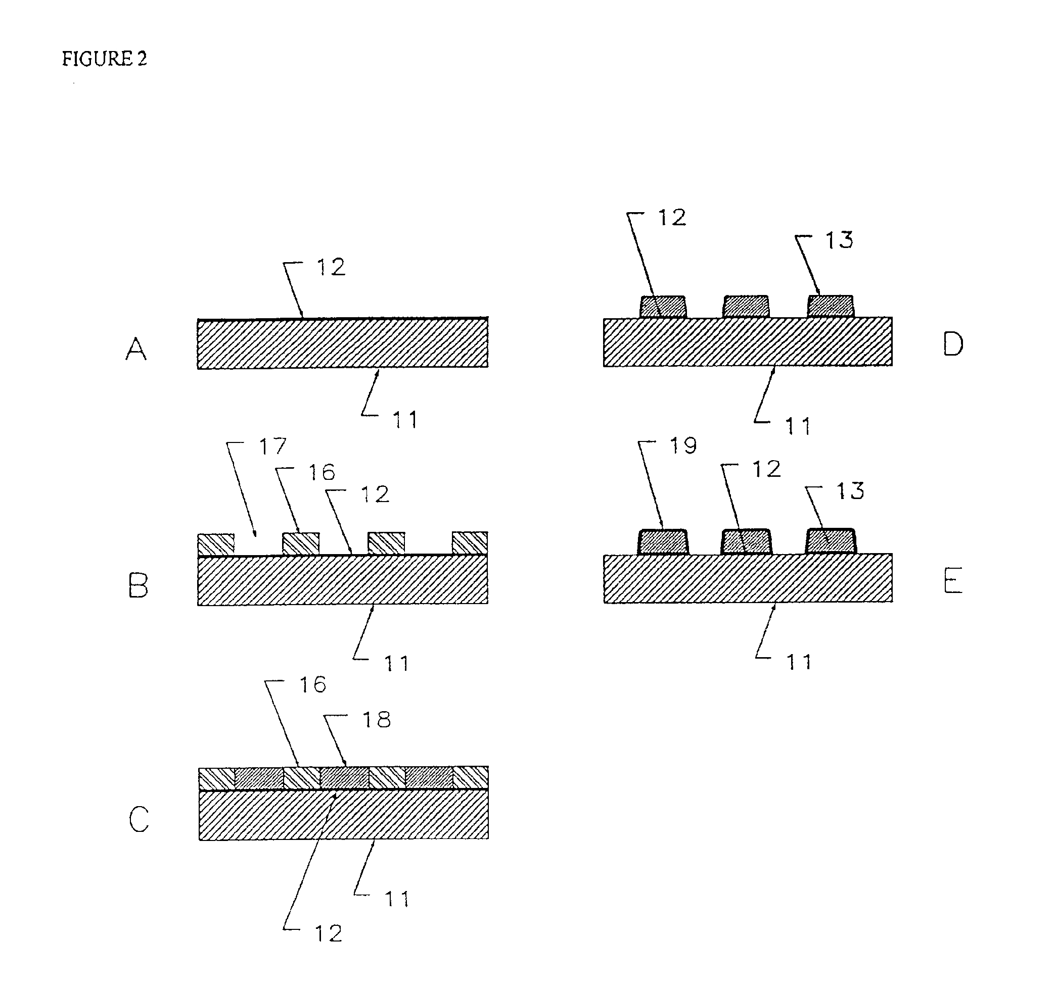
[0037]FIGS. 2A through 2E show the steps for an additive plating process used for fabricating a test probe. The probes ...


PUM


Abstract

A plated test probe structure for testing electrical connections to integrated circuits (IC) devices with solder bumped interconnection pads that are an integral part of the fan-out wiring on the test substrate, or other printed wiring device.

Description

[0001]This application claims the benefits of Provisional application Ser. No. 60 / 060 / 878, filed Oct. 2, 1991.FIELD OF THE INVENTION[0002]The present invention is directed to probe structures for testing of electrical interconnections to integrated circuit devices and other electronic components and particularly to testing of integrated circuit devices with solder bumped interconnection pads.BACKGROUND OF THE INVENTION[0003]Integrated circuit (IC) devices and other electronic components are normally tested to verify the electrical function of the device and certain devices require high temperature burn-in testing to accelerate early life failures of these devices. Wafer probing is typically done on a single chip site at temperatures ranging from 25° C.-125° C. while burn-in is typically done on diced and packaged chips at temperatures ranging from 80° C. to 150° C. Wafer probing and IC chip burn-in at elevated temperatures of up to 200° C. has several advantages and is becoming incr...

Claims


Application Information

Patent Timeline
IPC IPC(8): G01R1/067G01R1/073H05K3/24H05K3/32G01R1/06G01R31/26H01L21/66
CPCG01R1/06738G01R1/07314G01R1/0735G01R1/06761Y10T29/49169H05K3/244H05K3/325
Inventor BEAMAN, BRIAN SAMUELFOGEL, KEITH EDWARDLAURO, PAUL ALFREDO'SULLIVAN, EUGENE JOHNSHIH, DA-YUANTONG, HO-MING
Owner WL GORE & ASSOC INC
Why Eureka
Try Eureka