Method and device for atomic interferometry nanolithography

a nano-lithography and interferometer technology, applied in the field of lithography, can solve the problems of limited resolution and inflexible use of installation, and achieve the effect of reducing the contrast of rings

Inactive Publication Date: 2005-05-10
PARIS 13 UNIVERSITY
View PDF0 Cites 30 Cited by
  • Summary
  • Abstract
  • Description
  • Claims
  • Application Information

AI Technical Summary

Benefits of technology

[0011]More precisely, the invention provides a method of lithography by atomic interferometry on a target, on the basis: of spin polarizing a beam of incident atoms by optical pumping; of passing through a phase object by transverse magnetic induction acting on a coherent superposition of states; and then of analyzing the beam of atoms by optical interaction so as to retain only a single spin state, the emerging beam of atoms containing a series of interference terms; wherein the magnetic induction presents a transverse gradient to form an annular interference pattern, wherein the beam of atoms presents a speed distribution greater than 20% in order substantially to eliminate interference fringes other than the central fringe which then forms a spot, and wherein adjustable transverse uniform magnetic induction is added to the induction having a gradient so as to move the central spot in translation in predetermined manner over the target.
[0012]The use of a broad distribution of atom speeds, of the Maxwell type, causes contrast to drop off quickly with interference order, i.e. it reduces the contrast of the rings of the interference pattern outside the central spot.

Problems solved by technology

Thus, such an installation is not flexible in use.
In addition, the resolution that is obtained is limited by the performance of the mask used.

Method used


Image

  • Method and device for atomic interferometry nanolithography
  • Method and device for atomic interferometry nanolithography
  • Method and device for atomic interferometry nanolithography

Examples


Embodiment Construction

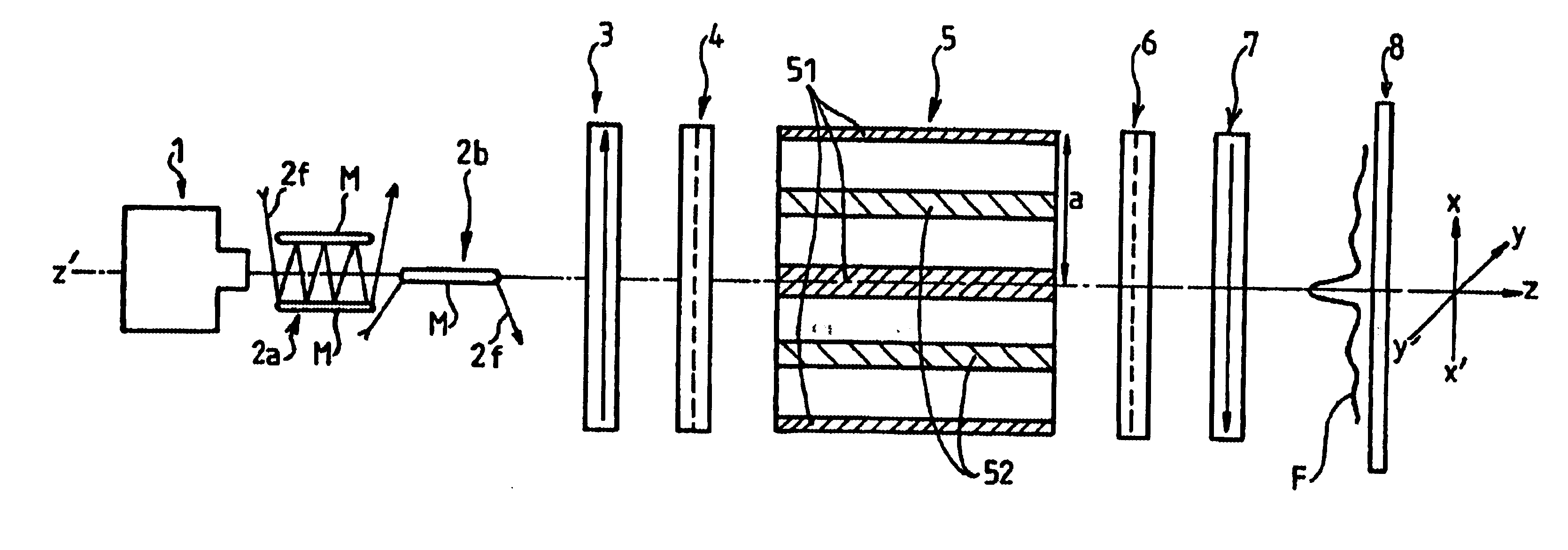
[0031]The nanolithography installation shown in FIG. 1 is based on a Stern-Gerlach type interferometer. The component elements of such an interferometer comprise in succession, along a central axis Z′-Z, a polarizer 3, a set of bars 51 producing a transverse magnetic field forming the phase object between two separator plates 4 and 6, followed by analyzer 7 and then a detector 8 which is located at the position on the substrate where deposition or etching is to take place.

[0032]The atomic interferometer receives a beam of metastable helium atoms He* delivered by a source 1. The source has a continuous electrical discharge triggered in expansion through a nozzle between a conical tungsten electrode and the nozzle. The discharge takes place at a voltage of about 1 kiloelectron volts (keV) and at a current of several milliamps (mA). Advantageously, the discharge can be pulsed and the resulting gas can be cooled, e.g. using liquid nitrogen.

[0033]The density at which atoms are delivered ...


PUM


Abstract

The invention proposes a novel technique for implementing high performance atomic lithography, and in particular high resolution lithography. The technique makes use of Stern-Gerlach type atomic interferometry enabling disturbances to be implemented in the atomic phase of the beam. Such interaction then directly modulates the intensity of the associated wave in the plane extending transversely to the beam of atoms, and does so in controllable manner. The installation of the invention for nanolithography by atomic interferometry comprises a Stern-Gerlach type interferometer comprising, as its phase object, four-pole magnetic induction having a transverse gradient created by four parallel bars carrying alternating direct currents, bracketed between two separator plates, preceded and followed respectively by a spin polarizer and by an analyzer operating by laser pumping. An additional uniform field is being created by another four additional bars powered in paired manner by adjustable currents in order to create a uniform field of arbitrary intensity and orientation for the interference pattern by adjusting the two current parameters. The source of atoms is a source that continuously discharges metastable helium or argon with approximately Maxwell type speed dispersion of about 30% to 40% in order to obtain a central spot.

Description

[0001]The invention relates to a method of performing lithography at nanometer scale by using atomic interferometry, and it also relates to an installation for implementing such a method.BACKGROUND OF THE INVENTION[0002]The invention relates to the field of lithography at sub-micron scale. By projecting beams of atoms either of alkali type (e.g. Na, Li, or Cr) or of metastable type (He* or Ar*), atomic lithography makes it possible, via a mask, respectively to cause substance to be deposited on a substrate to be treated or to cause a pattern to be etched in a resin deposited on that substrate. The article by M. Kreis et al., published in Applied Physics, Vol. B63, 649 (1996), illustrates that type of technique.[0003]Compared with the more conventional technique of photon lithography, atomic lithography presents advantages which relate to the implementation conditions and to the physical limits of these techniques:[0004]the photon source, generally a UV laser, requires high brightnes...

Claims


Application Information

Patent Timeline
Patent Type & Authority Patents(United States)
IPC IPC(8): H01J37/317
CPCB82Y10/00H01J37/3174B82Y40/00
Inventor BAUDON, JACQUESROBERT, JACQUES
Owner PARIS 13 UNIVERSITY
Why Eureka
Try Eureka