Semiconductor device having barrier layer between ruthenium layer and metal layer and method for manufacturing the same

a technology of ruthenium layer and barrier layer, which is applied in the direction of semiconductor devices, diodes, capacitors, etc., can solve the problems of poor surface characteristics between ruthenium layer and bonding layer or barrier layer

Inactive Publication Date: 2005-05-17
SAMSUNG ELECTRONICS CO LTD
View PDF10 Cites 85 Cited by
  • Summary
  • Abstract
  • Description
  • Claims
  • Application Information

AI Technical Summary

Problems solved by technology

However, if the bonding layer and the barrier layer are formed on a ruthenium layer, surface c

Method used


Image

  • Semiconductor device having barrier layer between ruthenium layer and metal layer and method for manufacturing the same
  • Semiconductor device having barrier layer between ruthenium layer and metal layer and method for manufacturing the same
  • Semiconductor device having barrier layer between ruthenium layer and metal layer and method for manufacturing the same

Examples


Embodiment Construction

[0027]Hereinafter, embodiments of the present invention will be described in detail with reference to the attached drawings. However, the embodiments of the present invention may be modified into various other forms, and the scope of the present invention must not be interpreted as being restricted to the embodiments. The embodiments are provided to more completely explain the present invention to those skilled in the art. In drawings, the thicknesses of layers or regions are exaggerated for clarity. Like numbers refer to like elements throughout. Also, when it is written that a layer is formed “on” another layer or a substrate, the layer may be formed directly on the other layer or the substrate, or other layers may intervene therebetween.

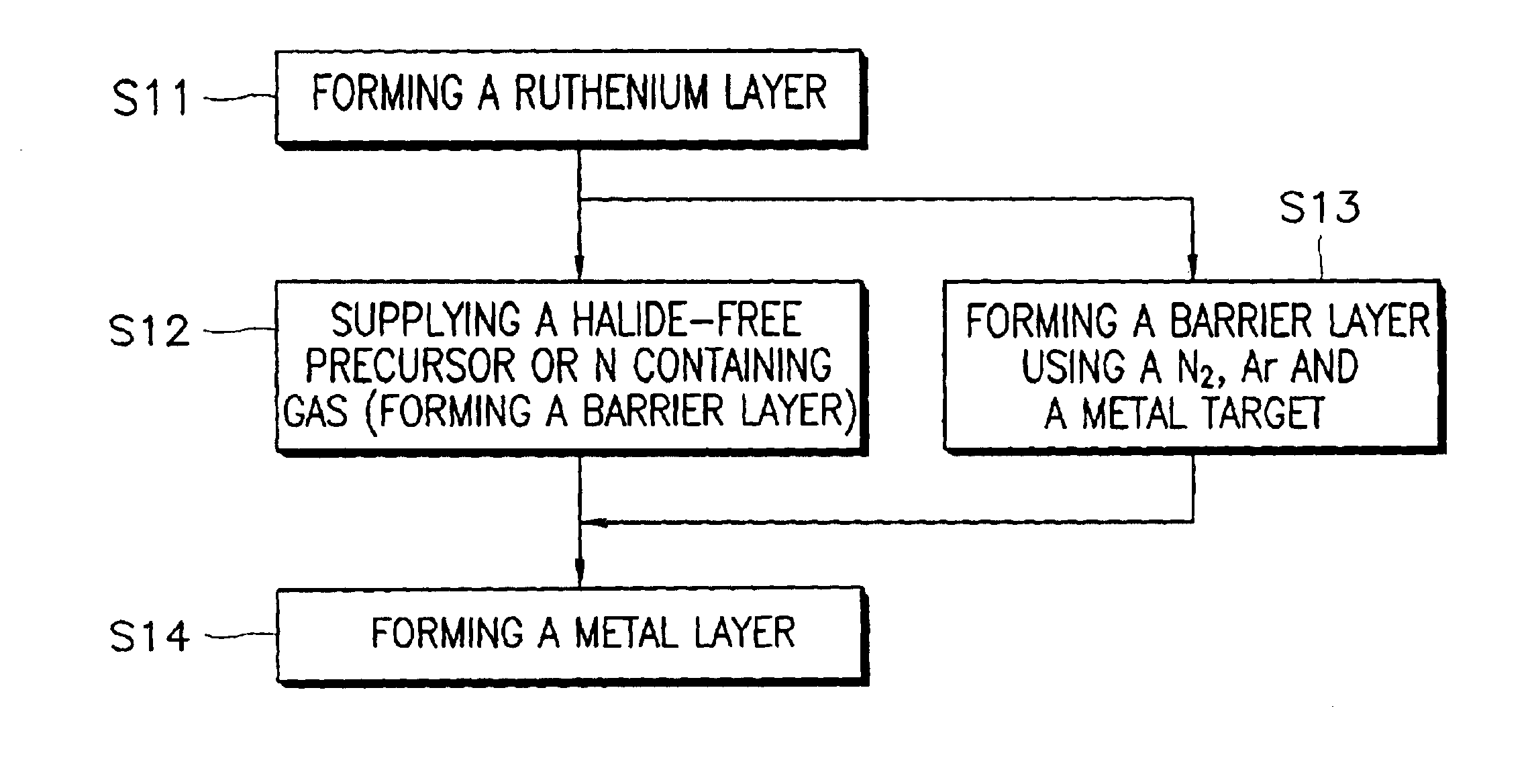
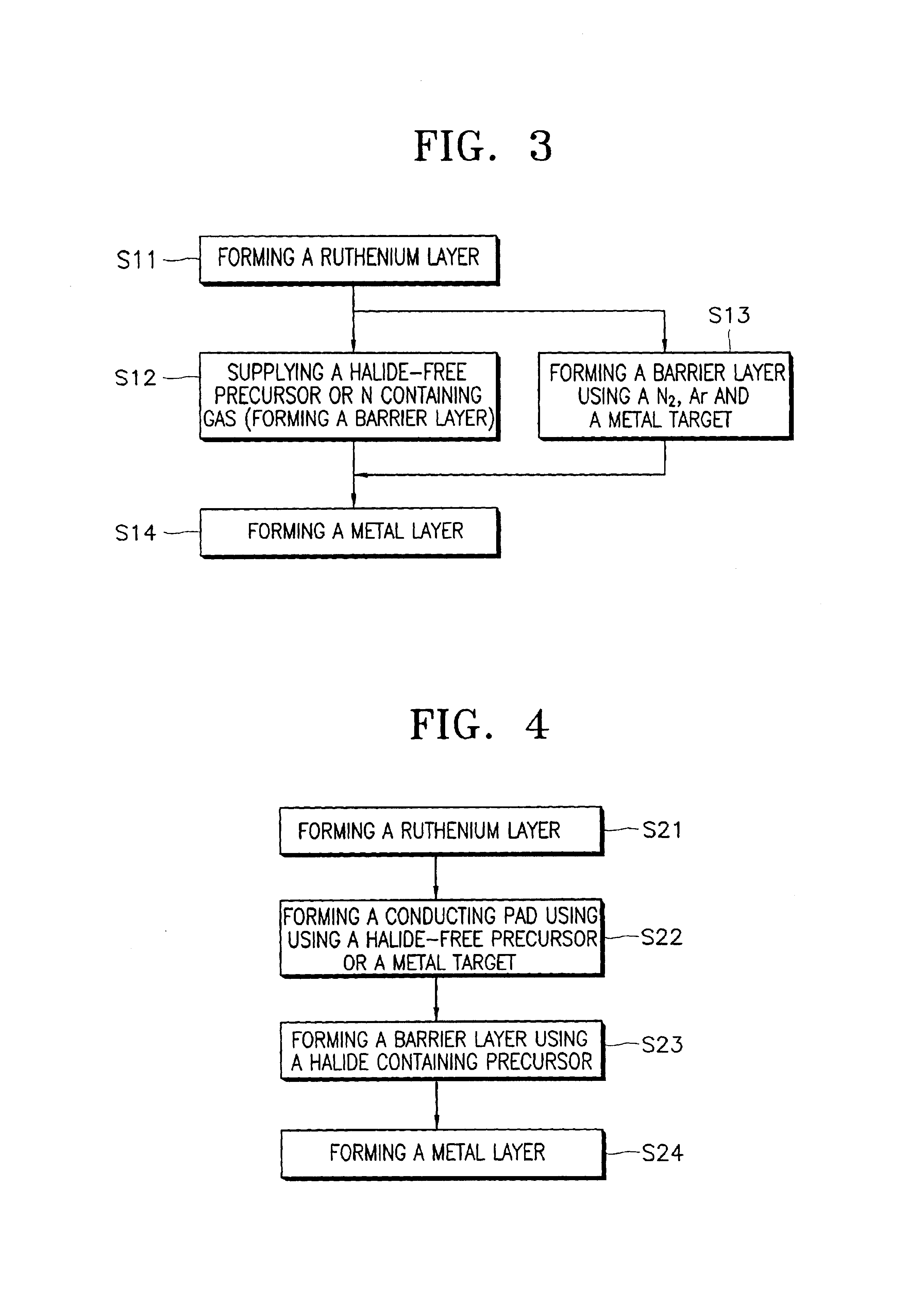
[0028]FIG. 3 shows a flow chart of a process for forming a barrier layer between a ruthenium layer and a metal layer according to an embodiment of the present invention. Referring to FIG. 3, a ruthenium layer is formed on a semiconductor substrate...


PUM


Abstract

A method for fabricating a semiconductor device is provided. A ruthenium layer is formed on a semiconductor substrate in a processing chamber. A barrier layer is formed on the ruthenium layer supplying a halide-free precursor in the processing chamber. A metal layer such as an aluminum layer, an aluminum alloy layer, a tungsten layer, or a copper layer is formed on the barrier layer. The barrier layer is one of a TiN layer, a TaN layer, a WN layer, and an MoN layer. The TiN layer is one of formed by using an MOCVD process and an ALD process, and the halide-free precursor is a titanium compound selected from the group consisting of pentakis(diethylamino) titanium, tetrakis(diethylamino) titanium, tetrakis(dimethylamino)titanium, and pentakis(dimethylamino)titanium. The TaN layer is formed by using one of an MOCVD process and an ALD process, and the halide-free precursor is a tantalum compound selected from the group consisting of t-butyltrikis(diethylamino)tantalum, pentakis(diethylamino)tantalum, tetrakis(dimethylamino)tantalum, and pentakis(dimethylamino)tantalum.

Description

BACKGROUND OF THE INVENTION[0001]1. Field of the Invention[0002]The present invention relates to a semiconductor device and a method for manufacturing the same, and more particularly, a semiconductor device having a barrier layer between a ruthenium layer and a metal layer and a method for manufacturing the same.[0003]2. Description of the Related Art[0004]Semiconductor memory devices generally include a plurality of conducting layers and a plurality of dielectric layers between the plurality of conducting layers. Among the plurality of the conducting layers, operatively related conducting layers are connected to each other. Generally, a bonding layer and a barrier layer are formed between a lower conducting layer and an upper conducting layer to prevent deterioration by physical and electrical differences between conducting layers such as separation and diffusion of impurities. The bonding layer and the barrier layer are typically formed between a silicon substrate and a bit line c...

Claims


Application Information

Patent Timeline
IPC IPC(8): H01L21/285H01L21/02H01L21/70H01L21/8242H01L21/768H01L27/105H01L27/06H01L27/108H01L27/04
CPCH01L21/28562H01L21/76843H01L27/0629H01L27/105H01L27/10894H01L28/75H01L28/90H01L27/10882H01L27/10814H10B12/315H10B12/48H10B12/09H01L27/04
Inventor PARK, HEE-SOOKCHOI, GIL-HEYUNLEE, SEUNG-HWANLEE, YUN-JUNG
Owner SAMSUNG ELECTRONICS CO LTD
Why Eureka
Try Eureka