Semiconductor device

a technology of semiconductor devices and on-resistance, which is applied in the direction of semiconductor devices, transistors, electrical devices, etc., can solve the problems of excessive increase in on-resistance, achieve the effect of preventing on-resistance from increasing, shortening the channel length, and increasing on-resistan

Inactive Publication Date: 2005-05-17
HITACHI LTD
View PDF2 Cites 25 Cited by
  • Summary
  • Abstract
  • Description
  • Claims
  • Application Information

AI Technical Summary

Benefits of technology

[0004]It is an object of the present invention to provide a structure that can attain a lower on-resistance and a better blocking effect.
[0008]In addition, because the insulating film and the auxiliary gate electrode are formed on the channel and the auxiliary gate electrode and the source electrode are shorted, the potential on the channel is fixed. The fixed potential prevents the depletion layer from being expanded from the drain at blocking time. This makes it possible to shorten the channel length, increases blocking performance, and attains low on-resistance.

Problems solved by technology

An attempt to ensure a predetermined withstand voltage in this way results in an excessive increase in the on-resistance.

Method used


Image

  • Semiconductor device
  • Semiconductor device
  • Semiconductor device

Examples


first embodiment

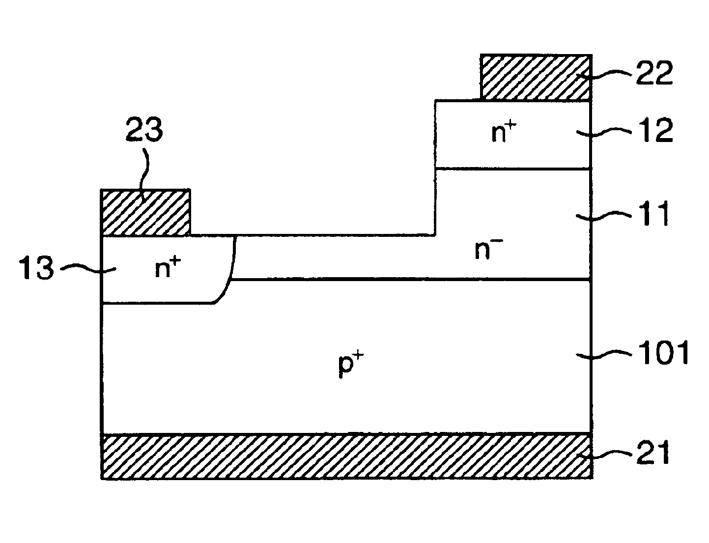
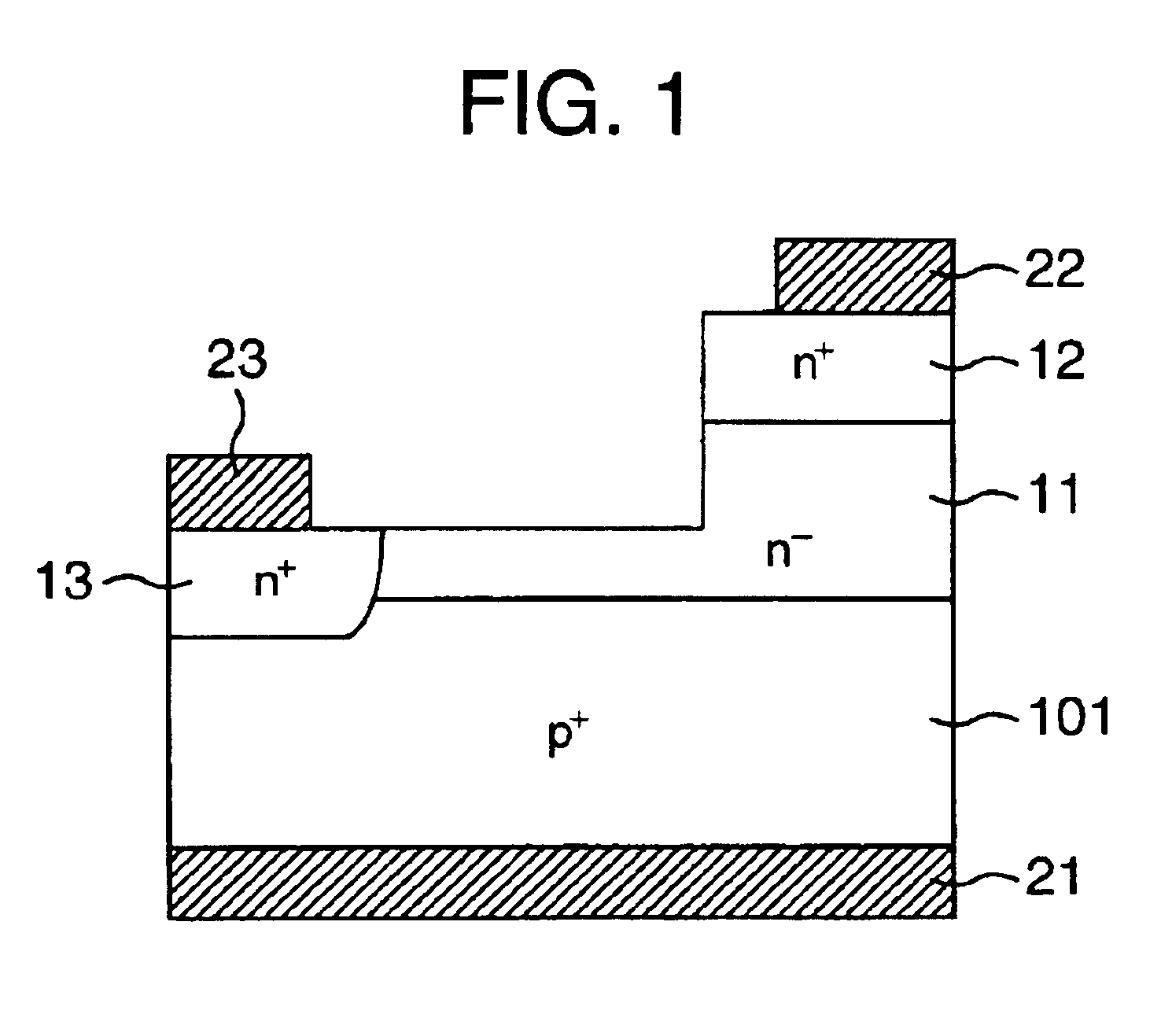
[0027]The present invention will be described below more in detail using some embodiments. FIG. 1 is a diagram showing the present invention and shows the cross sectional structure of a lateral channel type SIT. Referring to the figure, the numeral 101 indicates a p+ semiconductor body that is the gate region, the numeral 11 indicates an n− drift region, the numeral 12 indicates an n+ drain region, and the numeral 13 indicates an n+ source region. The numeral 21 indicates a gate electrode 21, the numeral 22 indicates a drain electrode, and the numeral 23 indicates a source electrode. In this embodiment, p-type 4H-SiC semiconductor body is used as the p+ gate region semiconductor body 101. An n epitaxial layer, 1.0 μm in thickness and 2.0×1017 cm−3 in density, is used as the drift region 11.

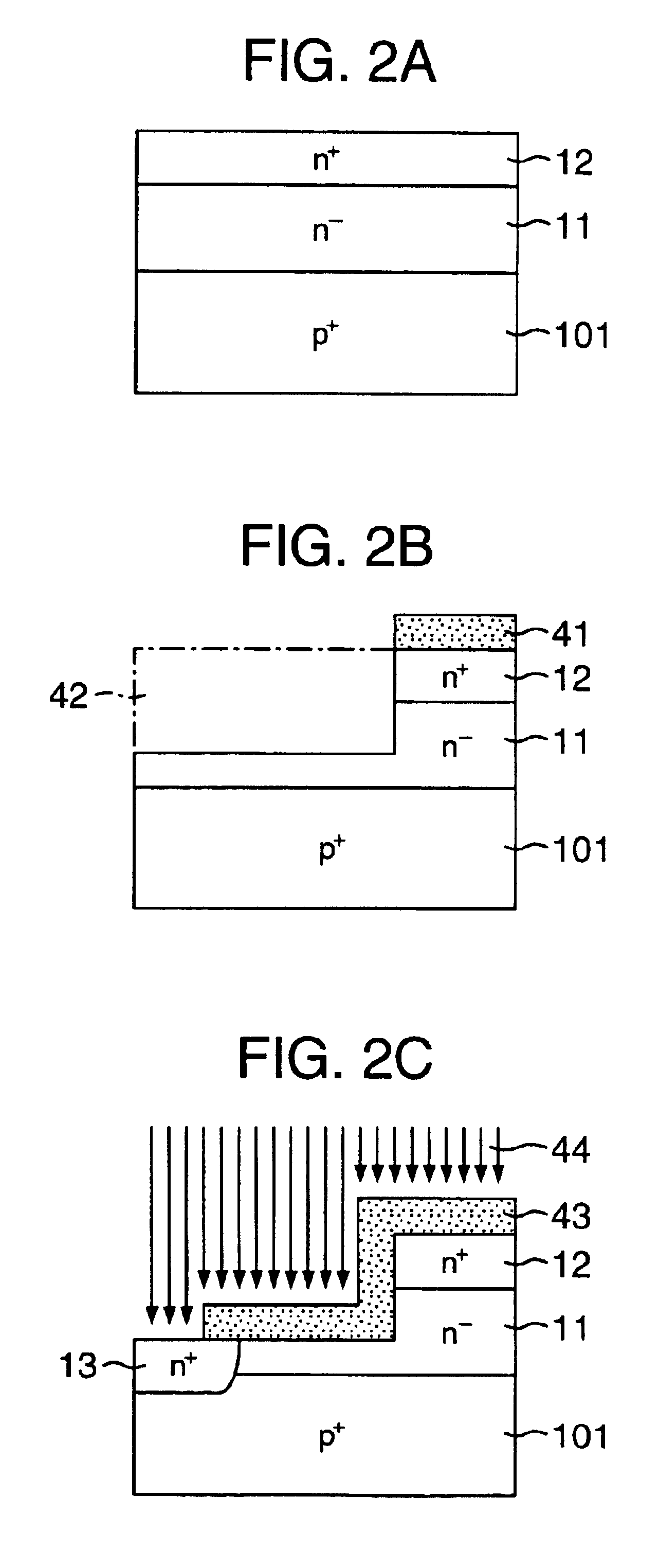
[0028]FIGS. 2A-2C are diagrams showing the fabrication process of the structure in this embodiment. As shown in FIG. 2A, the high-density n+ drain region 12 is epitaxially grown on the n− drift re...

second embodiment

[0031]FIG. 3 is a diagram showing the present invention and shows the cross sectional structure of a lateral type SIT. In this embodiment, ion implantation is used to form an n+ drain region 12. Like reference numerals in FIG. 1 are used to indicate like structural parts. This structure differs from that in FIG. 1 in that an n+ drain region 12 is formed on an n− drift region 11 through ion implantation. The junction end of the drain region 12 is exposed on the second major surface of the substrate that is an n− drift region 11.

[0032]FIGS. 5A-5C are diagrams showing the fabrication process of the second embodiment. After the n− drift region 11, 0.7 μm in thickness and 2.0×1017 cm−3 in density, is epitaxially grown on a p+ semiconductor body that is a gate region 101, a pattern is formed on a masking material 41 of SiO2 by the photolithography technology as shown in FIG. 5A and then a region 42 corresponding to the channel and the source is removed. Next, as shown in FIG. 5B, an n− ch...

seventh embodiment

[0043]FIG. 9 is a diagram showing the present invention and shows the cross sectional structure of a lateral type SIT. FIG. 11 is a perspective view of the semiconductor shown in FIG. 9. Like reference numerals in FIG. 9 are used to indicate like structural parts. In this embodiment, the depth is the long side. The top structure of the channel, integrated with the source electrode 23, increases the blocking effect in the off state. Therefore, it is desirable that this structure be formed across the channel width (depth direction) as in this embodiment.

[0044]Like reference numerals in FIG. 6 are used to indicate like structural parts. This embodiment is similar to the fourth embodiment except that a source electrode 23 extends into the direction of the channel such that the source electrode covers an SiO2 film 30 on the top of the channel. FIGS. 10A-10F show the formation process of this structure. As shown in FIG. 10A, a region 42 corresponding to the channel and the source is remov...


PUM


Abstract

A structure is provided that ensures a low on-resistance and a better blocking effect. In a lateral type SIT (Static Induction Transistor) in which a first region is used as a p+ gate and a gate electrode is formed on the bottom of the first region, the structure is built such that the p+ gate and an n+ source are contiguous. An insulating film is formed on the surface of an n− channel, and an auxiliary gate electrode is formed on the insulating film. In addition, the auxiliary gate electrode and the source electrode are shorted.

Description

BACKGROUND OF THE INVENTION[0001]The present invention relates to an improved structure of a lateral channel type junction type FET (JFET) or a static induction transistor (SIT).[0002]Silicon carbide (SiC), which has a dielectric breakdown field about 10 times as large as that of silicon (Si), is a material that reduces the loss because it can reduce the thickness, and increase the density, of the drift layer that withstands the voltage. Power semiconductor devices using SiC include a junction type FET (JFET) and a static induction transistor (SIT). An example of an SIT that utilizes the characteristics of SiC is the structure described in “Back-gate 4H-SiC JFET fabricated on n-type substrate” in Extended Abstracts for the 61st Autumn Meeting, 2000, The Japan Society of Applied Physics (September, 2000, Hokkaido Institute of Technology). The structure described in that publication is that the p+ layer, which is the gate region, is formed on the n-type substrate, the n− drift layer i...

Claims


Application Information

Patent Timeline
Patent Type & Authority Patents(United States)
IPC IPC(8): H01L21/02H01L29/74H01L21/337H01L29/66H01L29/808H01L31/0256H01L29/80H01L29/10H01L29/76H01L29/772
CPCH01L29/1066H01L29/808H01L29/7722H01L29/80
Inventor ONOSE, HIDEKATSUWATANABE, ATSUO
Owner HITACHI LTD
Why Eureka
Try Eureka