Operating a non-volatile memory device

a non-volatile memory and device technology, applied in the direction of static storage, digital storage, instruments, etc., can solve the problems of difficult to increase the surface area difficult to follow the processing of the memory device, complex patterning process of the floating gate, etc., to achieve the effect of improving the data retention characteristic and erasing the operation

Inactive Publication Date: 2005-05-17
SAMSUNG ELECTRONICS CO LTD
View PDF4 Cites 76 Cited by
  • Summary
  • Abstract
  • Description
  • Claims
  • Application Information

AI Technical Summary

Benefits of technology

[0011]Embodiments of the invention provide a method of operating a non-volatile memory device having SONOS cell transistors with...

Problems solved by technology

This can lead to difficulty in subsequent processing of the memory device.
Additionally, a process of patterning the floating gate is complicated and it is not easy to increase a surface area of the floating gate.
However, with a highly integrated non-volatile memory device, there are limitations in increasing the surface area of the floating gate.
That is, since the number of electrons injected into the charge trapping layer 7 through the blocking oxide layer 9 is greater than that ...

Method used


Image

  • Operating a non-volatile memory device
  • Operating a non-volatile memory device
  • Operating a non-volatile memory device

Examples


first embodiment

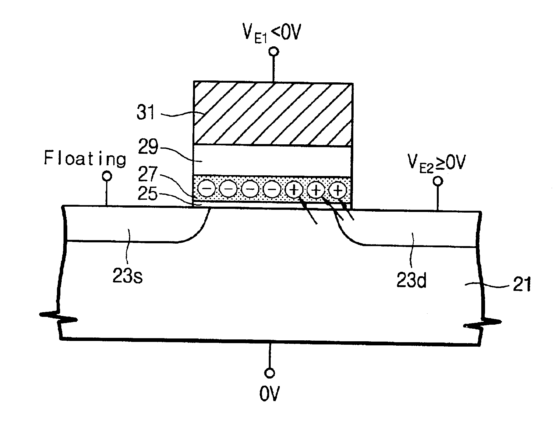
[0057]Referring to FIG. 4A, the first erasure voltage VE1 is applied to the gate electrode 31 of the SONOS cell transistor which has been programmed by the method explained in FIG. 3A. Also, the semiconductor substrate 21 is grounded, and the second erasure voltage VE2 is applied to the source region 23s. At this time, the drain region 23d is floating. Thus, differently from the first embodiment, holes are injected into the charge trapping layer 27 around the source region 23s by a source side injection.

[0058]FIG. 4B is a cross-sectional view for explaining a method of reading the erased SONOS cell transistor illustrated in FIG. 4A, according to another preferred embodiment of the present invention.

[0059]Referring to FIG. 4B, in the SONOS cell transistor that has been erased by the source side injection, an N-type channel inversion layer 22s is formed in the channel region around the source region 23s. The channel inversion layer 22s is formed by holes trapped in the charge trapping...

third embodiment

[0082]In the third embodiment, the second erasure voltage VE2 can be applied to all of the bit lines. In this case, all SONOS cell transistors Cj connected to the selected word line WLj are erased by the source and drain sides injection. That is, a page erasing operation is performed. Thus, in the event that the page erasing operation is performed through the source and drain sides injection, a read operation can be achieved using either the backward read mode or the forward read mode.

[0083]According to the erasing operations described in the first, second, and third embodiments of the present invention, it is impossible to simultaneously erase all cell transistors in one block. Thus, embodiments of the present invention additionally provide methods of simultaneously erasing all cell transistors in the block, and selectively programming at least one cell transistor out of the erased cell transistors in the block or all cell transistors connected to one word line. The erase methods, ...


PUM


Abstract

An operation method of programming, erasing, and reading a silicon-oxide-nitride-oxide-silicon (SONOS) non-volatile memory device having a tunnel oxide layer thicker than 20 Å is provided. A program operation of the method is accomplished by applying a program voltage higher than 0 volts and a ground voltage to a gate electrode and a channel region of a selected SONOS cell transistor, respectively. Also, an erasing operation is accomplished by applying a ground voltage and a first erase voltage lower than 0 volts to a bulk region and a gate electrode of a selected SONOS cell transistor, respectively, and by applying a second erasure voltage to either a drain region or a source region of the selected SONOS cell transistor. The second erase voltage is a ground voltage or a positive voltage. In addition, a read operation is accomplished using either a backward read mode or a forward read mode. Thus, it is possible to remarkably improve a bake retention characteristic, which is sensitive to a thickness of the tunnel oxide layer.

Description

RELATED APPLICATION[0001]This application relies for priority upon Korean Patent Application No. 2001-65030, filed on Oct. 22, 2001, the contents of which are herein incorporated by reference in their entirety.TECHNICAL FIELD[0002]This disclosure relates to operating a semiconductor device, and more particularly to a method of operating a non-volatile memory device having a silicon-oxide-nitride-oxide-silicon (SONOS) gate structure.BACKGROUND OF THE INVENTION[0003]Non-volatile semiconductor memory devices have a beneficial characteristic in that previous data are not erased although power is not supplied. Non-volatile memory devices are widely used in mobile telecommunication systems and computer memory cards.[0004]Generally, non-volatile memory devices include a stacked gate structure. The stacked gate structure includes a tunnel oxide layer, a floating gate, an inter-gate dielectric layer and a control gate electrode, which are sequentially stacked on a channel region of the cell ...

Claims


Application Information

Patent Timeline
IPC IPC(8): G11C16/04G11C16/10G11C16/26G11C16/06G11C16/14
CPCG11C16/0466G11C16/26G11C16/14G11C16/10G11C16/04
Inventor CHOI, JUNG-DALLEE, CHANG-HYUN
Owner SAMSUNG ELECTRONICS CO LTD
Why Eureka
Try Eureka