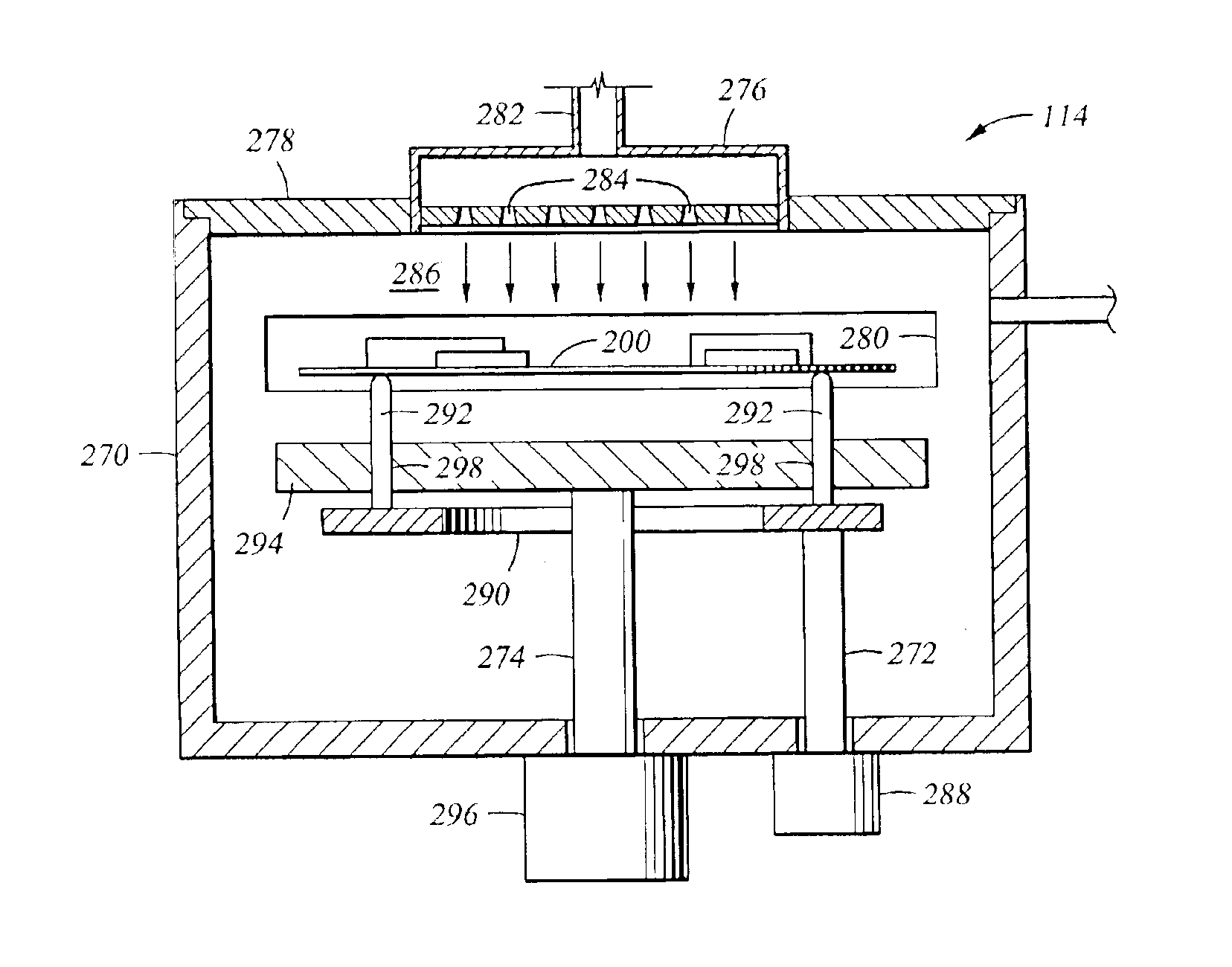
Additionally, the extremely fine and delicate nature of the circuits and other structures being constructed on the substrates may require that the processing system as a whole, and particularly each substrate support structure, be set as near to level as possible.
Failure to ensure that the processing system and / or each of the substrate support structures is properly level and / or aligned and is operating smoothly may cause damage to or improper processing of the substrates and can reduce the
throughput of the processing system since substrate exchanges may not be performed at maximum speed.
Relative alignment of the substrate support structures is typically more important than absolute leveling of the entire processing system since substrate exchange handling can result in significant slippage due to improper alignment.
When the substrate support structures, within a processing system, are improperly aligned, however, the support structures do not hold the substrates at about the same inclination, or tilt.
If substantial motion occurs prior to the remaining points making contact, then the substrate can slip.
In this manner, potentially contaminating particles may be scraped from the contacting points of the substrate causing backside
contamination of the substrate.
These particles may eventually work their way around to the top of the substrate and be deposited on the processed surface of the substrate, thereby contaminating the micro circuits or other structures constructed thereon.
An off-center substrate may undergo uneven or otherwise improper processing or may come in contact with surfaces or objects within the processing system that will contaminate the substrate, create potentially contaminating airborne particles or even break the substrate.
If the exchange is not coplanar, then the substrate will have the propensity to slip, resulting in misalignment and backside
contamination of the substrate.
When a processing system as a whole is improperly leveled, the system chambers, such as the transfer chamber, are inclined at an angle and can cause problems with the handling and processing of substrates and can exacerbate the problems with substrate support structures that are further inclined relative to the processing system.
Additionally, performance of certain functions that are sensitive to gravity may be affected by the inclination of the system.
When a transfer chamber substrate handler, for example, accelerates a substrate in a manner that may be appropriate for a level system, the substrate may, nevertheless, slide off-center due to the inclination, thereby exposing the substrate to potential damage from particles that may be generated by the slide or to potential collision with a surface or object in the processing system that requires a relatively close centering tolerance of the substrate for clearance.
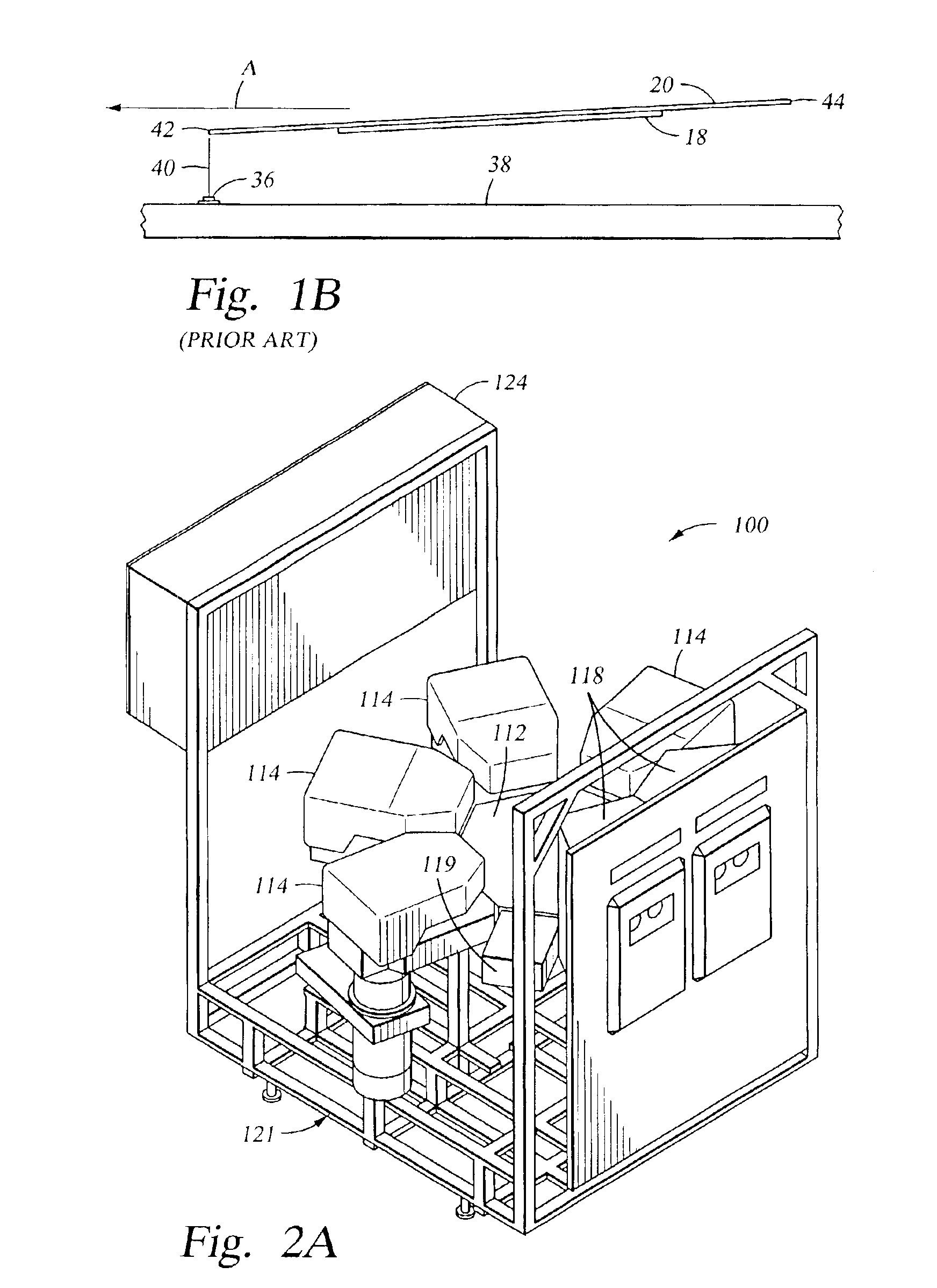
There are several problems with the measurement method depicted in FIG. 1a.
Therefore, the process chamber must also be opened, exposing the process chamber to possible
contamination and further increasing the down-time of the system.
Furthermore, the levels used to measure the inclination typically can resolve the inclination to within only two or three degrees accuracy, are highly dependent on the skill of the operator who is reading the level, and can affect the blade deflection due to the weight of the level, itself.
Therefore,
process systems or processes that are particularly sensitive to misalignment may be adversely affected.
Because of the problems and difficulties with performing this measurement method, some operators may elect not to make these measurements very thoroughly or even not to make them at all.
However, this method does not determine if the substrate 20 is level.
Moreover, since the
laser 36 is mounted into the processing system, removal of the
laser 36 is either impossible or very difficult.
Additionally, contaminants may prevent the proper functioning of the
optics.
Furthermore, a warped substrate may lead the
laser sensors to incorrectly determine that the blade or substrate is inclined.
Therefore, although this method can be performed without opening the processing system, this method is very inflexible.
Thus, over time, the blade 18 may be warped out of alignment, so the blade 18 may degrade and hold the substrates at an unacceptable inclination.
Other shifting of alignments between the various substrate support structures, due to the wear or slippage from
constant movement during processing, may also occur.
Because of the down-time associated with the method shown in FIG. 1a, many operators elect not to perform the method or to wait until the substrate support structures are severely out of alignment and potentially damaging the substrates.

