Semiconductor device and an information management system thereof

a technology of information management system and semiconductor, applied in the direction of semiconductor/solid-state device testing/measurement, instruments, sensing by electromagnetic radiation, etc., can solve the problem of limited information that can be recorded using alphanumeric characters, large number of complicated processes to be implemented, dirt and scarring, etc., to achieve a high degree of flexibility

Inactive Publication Date: 2005-05-24
HPLP TECH
View PDF11 Cites 27 Cited by
  • Summary
  • Abstract
  • Description
  • Claims
  • Application Information

AI Technical Summary

Benefits of technology

[0025]As explained above, by using the chip ID information, the frame ID information and the product ID information that are coded through two-dimensional code patterns in the inter-process physical distribution during the semiconductor manufacturing processes, detailed management can be implemented for individual chips, thereby making it possible to establish a semiconductor manufacturing facility that is capable of supporting production of many different types of products in small quantities with a...

Problems solved by technology

As explained above, an extremely large number of complicated processes must be implemented to complete the semiconductor device, and it is necessary to implement accurate information management in regard to the information on the semiconductor product in the individual processes.
However, there is a limit to the quantity of information that can be recorded using alphanumeric characters.
Furthermore, it is necessary to perform edge recognition processing when reading alphanumeric characters, which is difficult.
There is an added problem with this method, in that it is vulnerable to dirt and scarring.
However, there is a limit to the quantity of information that can be recorded in a one-dimensional code pattern per unit area,...

Method used


Image

  • Semiconductor device and an information management system thereof
  • Semiconductor device and an information management system thereof
  • Semiconductor device and an information management system thereof

Examples


Embodiment Construction

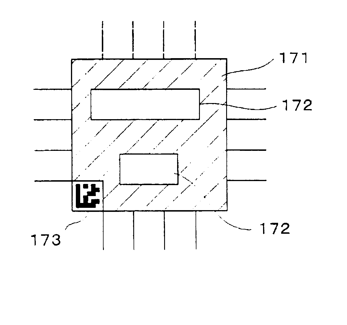
[0050]The following is a detailed explanation of preferred embodiments of the semiconductor device and the information management system therefor according to the present invention in reference to the attached drawings.

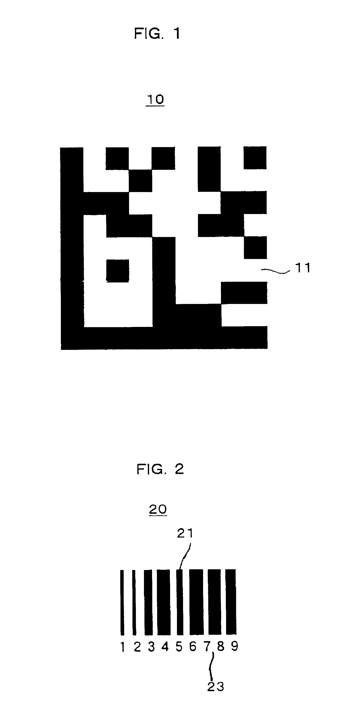
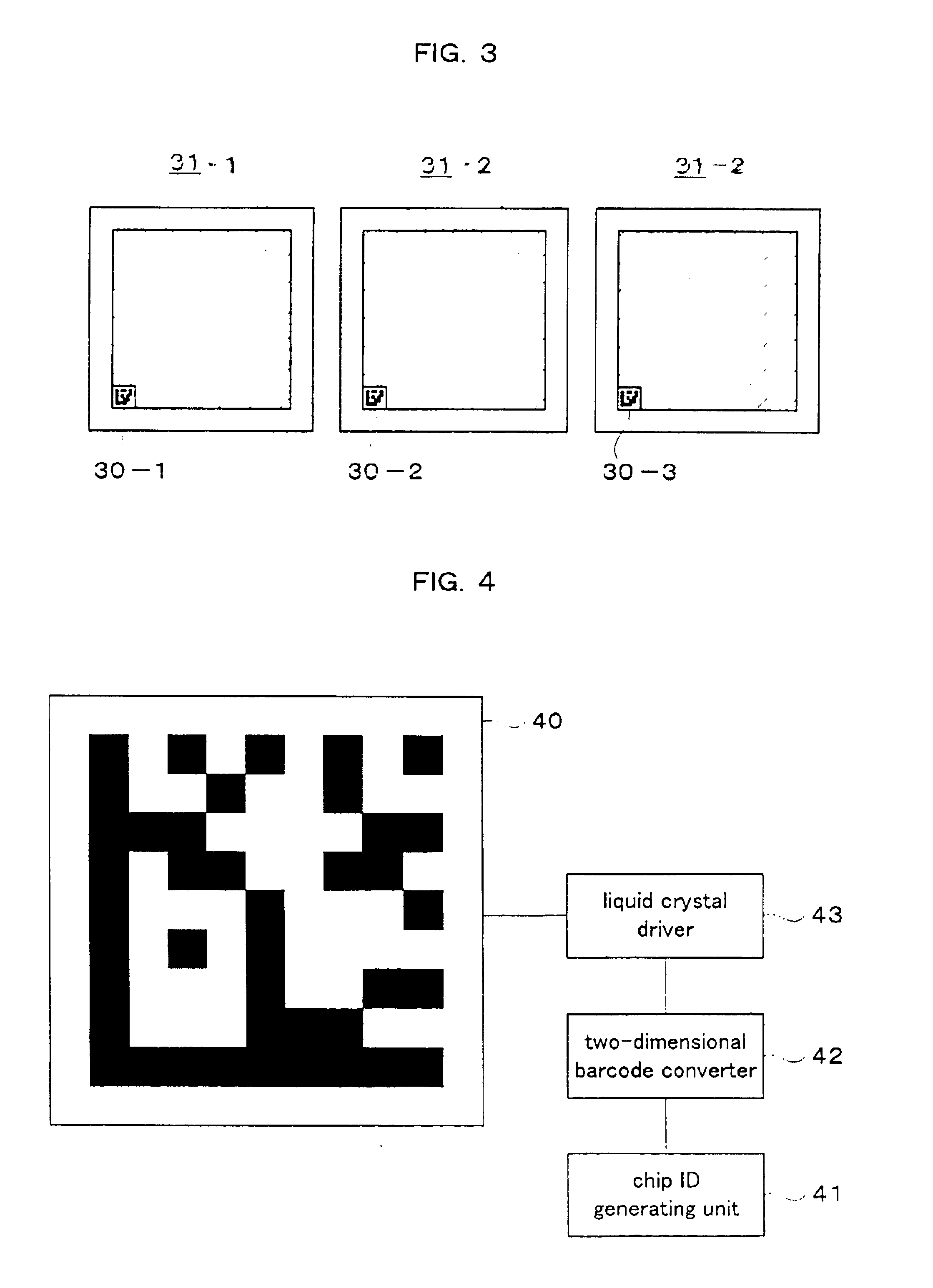
[0051]First, in FIG. 1, an example of a two-dimensional code pattern and in particular a two-dimensional barcode pattern which may be employed in an embodiment of the present invention is shown. As shown in the figure, a two-dimensional barcode code pattern 10 is a two-dimensional pattern in which specific information can be recorded by coloring the squares 11 of a grid in black or white to form blocks that extends two-dimensionally in conformance to predetermined rules. It is to be noted that while the encoding rules for coloring the grid black and white in the two-dimensional pattern may be the same as those in the prior art, new encoding rules may be created instead. A detailed explanation of the actual method for coloring the grid black and white is omitted since ...


PUM


Abstract

Individual two-dimensional barcodes 30, 91 and 173 are provided for individual chips 31 arrayed on a wafer 50, individual lead frames 93 to each of which chips 92 are bonded and individual packaged products 171 constituted of resin sealed semiconductor chips based upon chip ID information to enable information management to be implemented separately for individual chips 31, individual frames 93 and individual chip products 171. Thus, a higher degree of efficiency and a higher degree of accuracy in the information management for semiconductor devices are achieved in all processes of semiconductor production including the individual manufacturing processes, the physical distribution process, the shipping process and the claim handling process.

Description

BACKGROUND OF THE INVENTION[0001]1. Field of the Invention[0002]The present invention relates to a semiconductor device and an information management system for this semiconductor device, and in particular, it relates to a semiconductor device and an information management system therefor that achieve implementation of efficient and accurate information management with regard to the production processes for manufacturing the semiconductor device by utilizing a two-dimensional bar code pattern.[0003]2. Description of the Related Art[0004]A manufacturing method for manufacturing semiconductor devices normally consists of an extremely large number of processes. In a typical manufacturing method for producing semiconductor devices, first, during the wafer processing process, a photolithography step, an etching step, a washing step and the like are performed repeatedly on the surface of the wafer to form the required semiconductor chips. Next, testing for a pass / fail assessment of the in...

Claims


Application Information

Patent Timeline
IPC IPC(8): H01L23/544G01R31/26H01L21/02H01L21/66H01L23/50
CPCG06K1/126G06Q10/08H01L23/544H01L24/85H01L24/78H01L2224/49171H01L2224/7865H01L2924/3025Y10S235/90H01L24/49H01L2224/78901H01L2224/85H01L2924/01004H01L2924/01012H01L2924/01014H01L2924/01075H01L2924/01082H01L2924/14H01L2924/1433H01L2223/54413H01L2223/54433H01L2223/54473H01L2223/5448H01L2223/54486H01L2224/48H01L24/48H01L2924/00014H01L2924/01005H01L2924/01006H01L2924/01033H01L2224/78H01L2924/00H01L2224/05554H01L2924/12042H01L2224/45099H01L2224/05599H01L21/027
Inventor KUDO, ISAO
Owner HPLP TECH
Why Eureka
Try Eureka