Eureka AIR delivers breakthrough ideas for toughest innovation challenges, trusted by R&D personnel around the world.

Electromagnetic window

Inactive Publication Date: 2005-05-24
ANAFA ELECTROMAGNETIC SOLUTIONS
View PDF16 Cites 7 Cited by
  • Summary
  • Abstract
  • Description
  • Claims
  • Application Information

AI Technical Summary

Benefits of technology

[0020]Owing to the fact that the elements are small in size relative to the wavelength (or wavelengths) of the radiation propagating in the dielectric structure, no self-resonance of the individual inclusion is excited within the frequency band to be transmitted. The dimensions of the radiation scattering elements and spaces between them are chosen such that the scattering from the elements compensates for the reflection from the dielectric discontinuities (e.g., the air-dielectric interfaces), thereby causing the formation of a double-resonance transmission band. More specifically, in the case of a single dielectric layer, the two transmission peaks of the unloaded window at frequencies related to the half-wavelength and one-wavelength of the electromagnetic radiation are both brought close to the three-quarter-wavelength point, and generate together a deep and wide transmission band. For example, a typical bandwidth at the −20 dB level is 5 times wider than that of the conventional half-wavelength window.
[0027]The device may also utilize thin layers of ferroelectric materials of very high dielectric constant controlled by an external voltage source (in a symmetrical position relative to the layer(s) of metal objects). This allows a gradual change of the average dielectric constant, and the dynamic shift of the location of the pass-band according to the applied voltage. The above-indicated strips made of an electrically conductive material may be used, being printed on one or two sides of these ferroelectric layers to thereby enable application of a DC voltage to the ferroelectric layers.
[0028]The window structure according to the invention is mildly dependent on the angle of incidence at angles up to 60 degrees, for both parallel and perpendicular polarizations. Hence, the device is characterized by improved transmission, as compared to that of the conventional half-wavelength window. This effect is achieved by controlling both the array grid parameters and the size of the conductive inclusions. The use of different combinations of grid parameters and inclusions' size result in the same transmission curve at normal incidence, while differing appreciably in oblique incidence transmission (i.e., the denser the grid, the milder the effects of oblique incidence).
[0029]The device according to the invention may be a multi-stage structure, where dielectric structures, each with the two-dimensional array of metal-containing inclusions, are placed on top of each other. Several structures constructed as described above can be combined to generate a thick multi-stage window structure with very sharp transitions at the frequency edges of the transmission band, at the expense of higher transmission loss.
[0030]The performance of the multi-stage structure may be improved by varying the layers' thicknesses (in a symmetric layer structure) and dimensions of the conducting solids, wherein the transmission response curve is tuned as a function of frequency. The stages (each in the form of the above-described structure) can be shifted laterally by half the grid constants to generate new three-dimensional grids out of the same two-dimensional grids.

Problems solved by technology

Actually, an attempt to operate at the resonance frequency of the element would result in the total reflection of the electromagnetic wave.

Method used


Image

  • Electromagnetic window
  • Electromagnetic window
  • Electromagnetic window

Examples


Embodiment Construction

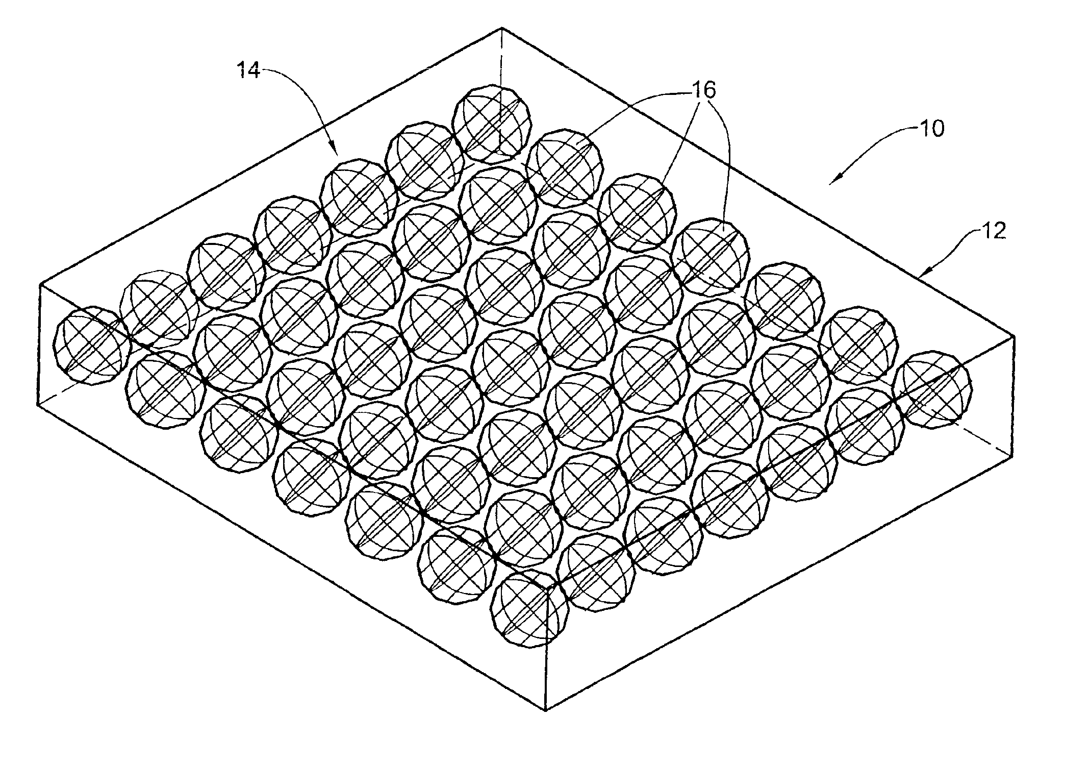
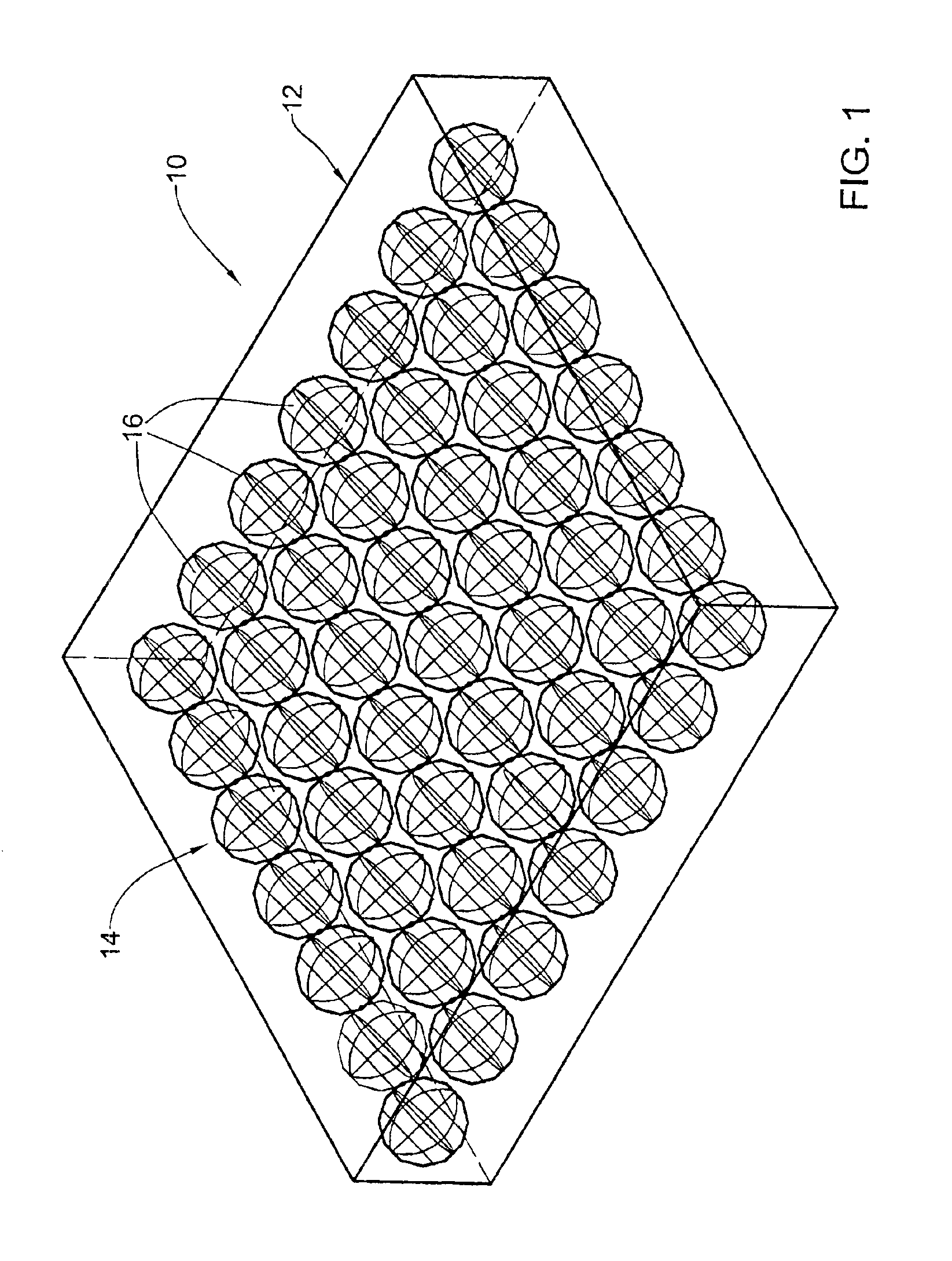
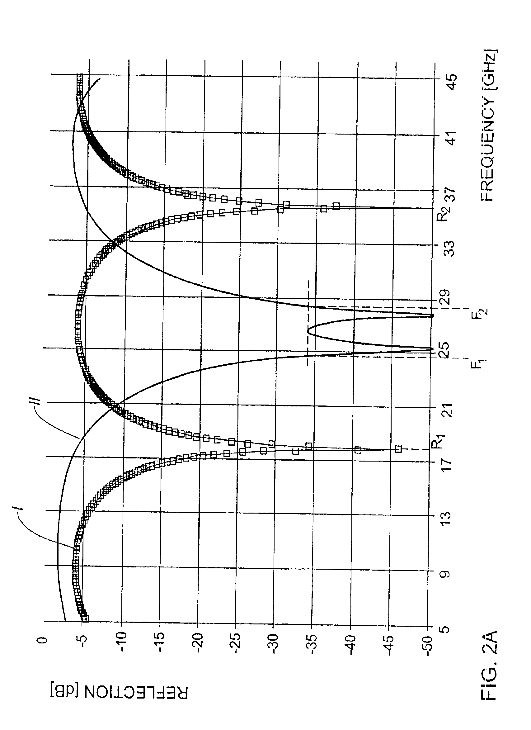
[0057]Referring to FIG. 1, there is illustrated a device 10 according to the invention, presenting a single layer window for transmitting therethrough electromagnetic radiation of the wavelength λ0 (or a wavelength band with the central wavelength λ0). The device 10 comprises a dielectric structure 12 (single dielectric layer slab in the present example) and an inner two-dimensional periodic pattern 14 (grid) located inside the slab defining a patterned area. The pattern 14 is formed by sub-resonant capacitive metal inclusions 16 (constituting elements capable of scattering incident radiation), which are aligned in a disconnected from each other spaced-apart relationship with a grid constant a in a central plane of the slab 12. In the present example, such inclusions are spheres with a radius r.

[0058]It should be noted that the inclusions can be made of metal elements, metal-coated dielectric elements, or dielectric-coated metal element. In cases where the inclusions are closely pac...


PUM


Abstract

Ad device substantially transparent to electromagnetic radiation of a certain frequency band is presented. The device comprises at least one dielectric structure of a predetermined thickness defined by the central frequency of the operational frequency band of the device, and comprises a predetermined substantially periodic inner pattern inside the dielectric structure composed of a two-dimensional array of substantially identical sub-resonant capacitive elements made of an electrically conducting material and capable of scattering said electromagnetic radiation arranged in a disconnected from each other spaced-apart relationship.

Description

FIELD OF THE INVENTION[0001]This invention is generally in the field of electromagnetics, and relates to a device that presents an electromagnetic window allowing electromagnetic radiation of various frequencies to pass therethrough. The invention is particularly useful in radomes that cover antennas in the RF, microwaves, millimeter waves and sub-millimeter waves frequency bands; and in optical devices where the transmission of infrared, visible and ultraviolet frequency bands is required.BACKGROUND OF THE INVENTION[0002]Electromagnetic windows are usually designed to cover and protect a radiation source while maintaining high transmission of the radiation generated thereby, and are typically based on one or more planar or shaped dielectric layers. Electromagnetic windows can be divided into two groups: all-dielectric and metal-dielectric.[0003]The all-dielectric windows are built from either a single dielectric layer or multiple dielectric layers, designed to maximize the transmis...

Claims


Application Information

Patent Timeline
IPC IPC(8): H01Q15/00H01Q17/00
CPCH01Q15/0013H01Q17/00
Inventor FRENKEL, AVRAHAM
Owner ANAFA ELECTROMAGNETIC SOLUTIONS
Why Eureka
Eureka Blog
Learn More