
Coupled cavity high power semiconductor laser

a semiconductor laser and coupled cavity technology, applied in semiconductor lasers, optical resonators, instruments, etc., can solve the problems of significant limitations, limited practical output power of such a device, and inability to meet the requirements of commercial manufacture or use, and achieves greater device efficiency and power levels. high

Inactive Publication Date: 2005-05-24
NECSEL INTPROP +1
View PDF10 Cites 59 Cited by
  • Summary
  • Abstract
  • Description
  • Claims
  • Application Information

AI Technical Summary

Benefits of technology

The device achieves significantly higher power output in a single spatial mode with improved efficiency, allowing for practical and manufacturable high-power operation, with the substrate's higher doping level reducing electrical resistance without increasing optical loss.

Problems solved by technology

Conventional vertical cavity surface-emitting lasers (VCSELS) typically have two flat resonator cavity mirrors formed onto the two outer sides of a layered quantum-well gain structure, and are significantly limited in single spatial-mode output power, typically a few milliwatts.
While greater optical power can be achieved from conventional VCSEL devices by using larger emitting areas, such a large aperture device is not particularly practical for commercial manufacture or use, and produces an output which is typically distributed across many higher order spatial modes.
Since any heat produced in the active gain region must be removed through the relatively thick p-type substrate, the practical output power from such a device is limited to about 100 mw for pulsed operation and to only a few mw for continuous (“cw”) operation.
However, especially in an electrically pumped device with a relatively thick substrate inside the laser cavity, increasing the doping of the substrate (desirable to minimize carrier crowding and electrical resistance) also increases the optical loss at the laser wavelength and the overall efficiency of the device is correspondingly reduced.

Method used


Image

  • Coupled cavity high power semiconductor laser
  • Coupled cavity high power semiconductor laser
  • Coupled cavity high power semiconductor laser

Examples


Embodiment Construction

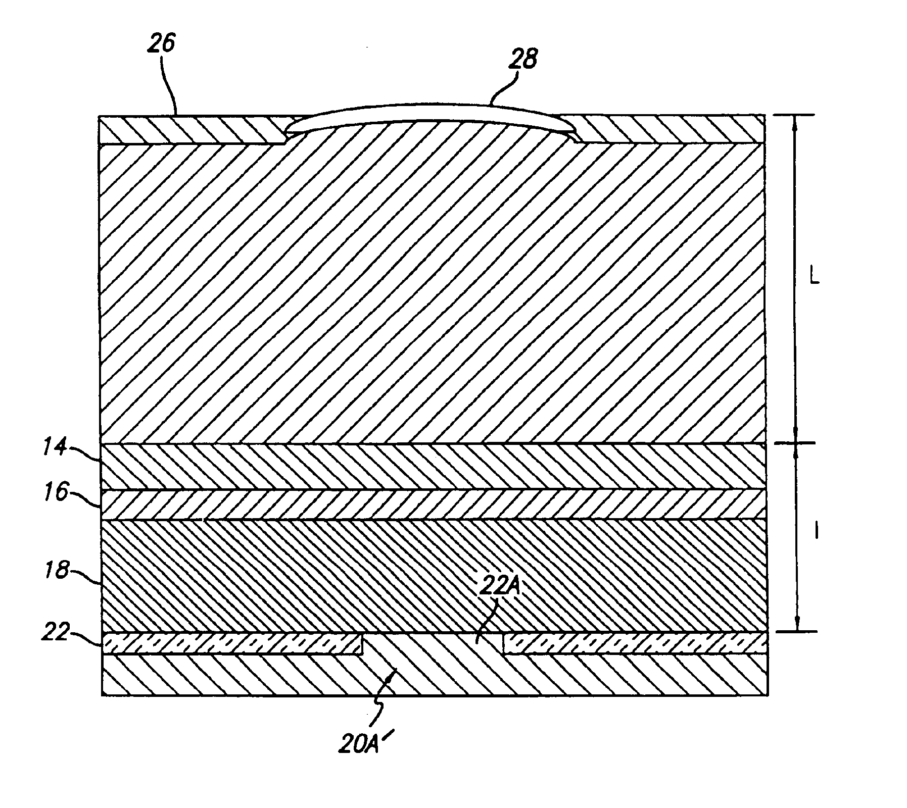
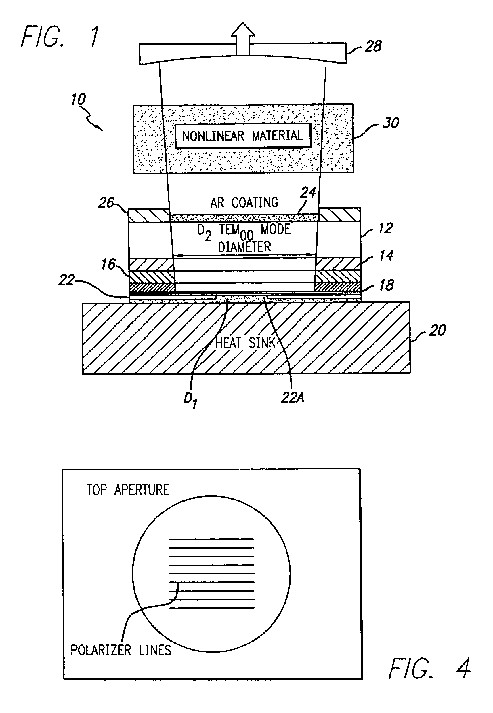
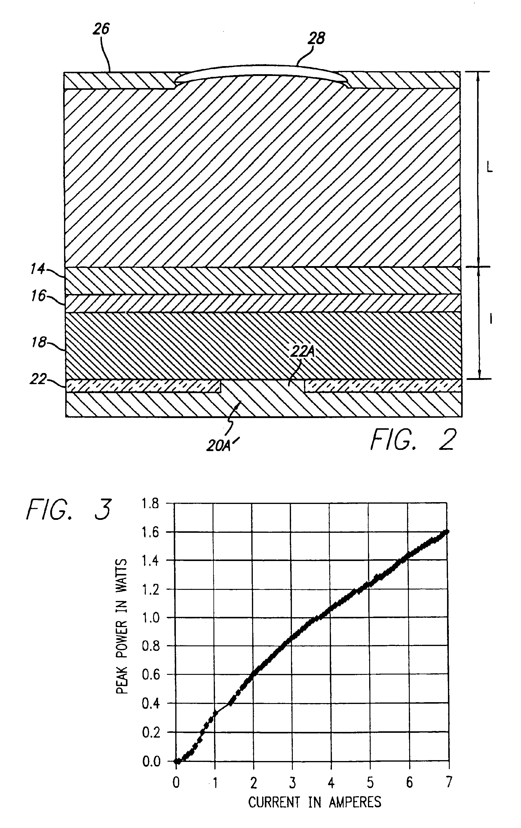
[0024]A preferred embodiment of a coupled cavity VECSEL 10 according to the present invention is shown schematically in FIG. 1. The coupled cavity VECSEL 10 includes an n-type semiconductor substrate 12. The substrate 12 of the present invention should be sufficiently thick to be conveniently handled during manufacturing process and is sufficiently doped with n-type dopants to reduce the electrical resistance of substrate 12 to a value required for efficient operation and nearly uniform carrier injection across the current aperture region at high power levels (so that the active gain region is pumping uniformly without excessive carrier crowding), but without a corresponding sacrifice of the optical efficiency, as will be explained in detail in the following paragraphs. In an exemplary embodiment, the current aperture diameter is 100 μm and the doping level of the n-type dopants in the substrate is approximately between 1×10⁻¹⁷ cm−3 and 5×10⁻¹⁷ cm−3; the substrate is approximately 5...


PUM

PropertyMeasurementUnit
reflectivityaaaaaaaaaa
current aperture diameteraaaaaaaaaa
thickaaaaaaaaaa

Abstract

An active gain region sandwiched between a 100% reflective bottom Bragg mirror and an intermediate partially reflecting Bragg mirror is formed on a lower surface of a supporting substrate, to thereby provide the first (“active”) resonator cavity of a high power coupled cavity surface emitting laser device. The bottom mirror is preferably in direct thermal contact with an external heat sink for maximum heat removal effectiveness. The reflectivity of the intermediate mirror is kept low enough so that laser oscillation within the active gain region will not occur. The substrate is entirely outside the active cavity but is contained within a second (“passive”) resonator cavity defined by the intermediate mirror and a partially reflecting output mirror, where it is subjected to only a fraction of the light intensity that is circulating in the gain region. The active gain region is preferably electrically excited, with a circular bottom electrode formed by an oxide current aperture between the bottom mirror and the heat sink, and with an annular top electrode formed on an upper surface of the substrate.

Description

[0001]This is a Divisional Application of U.S. application Ser. No. 09 / 519,890, filed Mar. 6, 2000, now U.S. Pat. No. 6,778,582.FIELD OF THE INVENTION[0002]This invention relates generally to an electro-optical device and, more particularly, to a surface-emitting semiconductor laser.BACKGROUND OF THE INVENTION[0003]Conventional vertical cavity surface-emitting lasers (VCSELS) typically have two flat resonator cavity mirrors formed onto the two outer sides of a layered quantum-well gain structure, and are significantly limited in single spatial-mode output power, typically a few milliwatts. While greater optical power can be achieved from conventional VCSEL devices by using larger emitting areas, such a large aperture device is not particularly practical for commercial manufacture or use, and produces an output which is typically distributed across many higher order spatial modes. Several schemes have been proposed for increasing single-model output power from surface-emitting device...

Claims


Application Information

Patent Timeline
Patent Type & Authority Patents(United States)
IPC IPC(8): H01S5/00H01S5/183H01S5/40H01S5/42H01S3/106H01S3/107H01S3/109H01S5/06H01S5/065H01S5/10H01S5/14G02F1/017G02F1/03
CPCH01S5/18311H01S3/109H01S5/0207H01S5/1021H01S5/141H01S2301/166H01S5/18355H01S5/18386H01S5/18388H01S5/423
Inventor MOORADIAN, ARAM
Owner NECSEL INTPROP
Learn More