Method of manufacturing electron-emitting device using ink-jet discharge device

a technology of electron emission and inkjet discharge, which is applied in the manufacture of resistive materials, electrode systems, electric discharge tubes/lamps, etc., can solve the problems of reducing the yield of an electron source substrate, increasing production costs, and difficult to increase the yield of an electronic device, so as to prevent unwanted short-circuiting, improve the reproducibility of characteristics, and uniform electron emission characteristics

Inactive Publication Date: 2005-06-07
CANON KK
View PDF16 Cites 13 Cited by
  • Summary
  • Abstract
  • Description
  • Claims
  • Application Information

AI Technical Summary

Benefits of technology

[0062]By these apparatus and method, the present invention can discharge a solution to an accurate position on a substrate, and can manufacture an electronic device excellent in reproducibility of characteristics.
[0063]By these apparatus and method, the present invention can discharge a solution to an accurate position on a substrate, and can manufacture an electron source having a plurality of electron-emitting portions with uni

Problems solved by technology

However, forming the building component of the electronic device using the ink-jet method suffers the following problems.
Hence, the yield in manufacturing an electronic device is difficult to increase

Method used


Image

  • Method of manufacturing electron-emitting device using ink-jet discharge device
  • Method of manufacturing electron-emitting device using ink-jet discharge device
  • Method of manufacturing electron-emitting device using ink-jet discharge device

Examples


first embodiment

(First Embodiment)

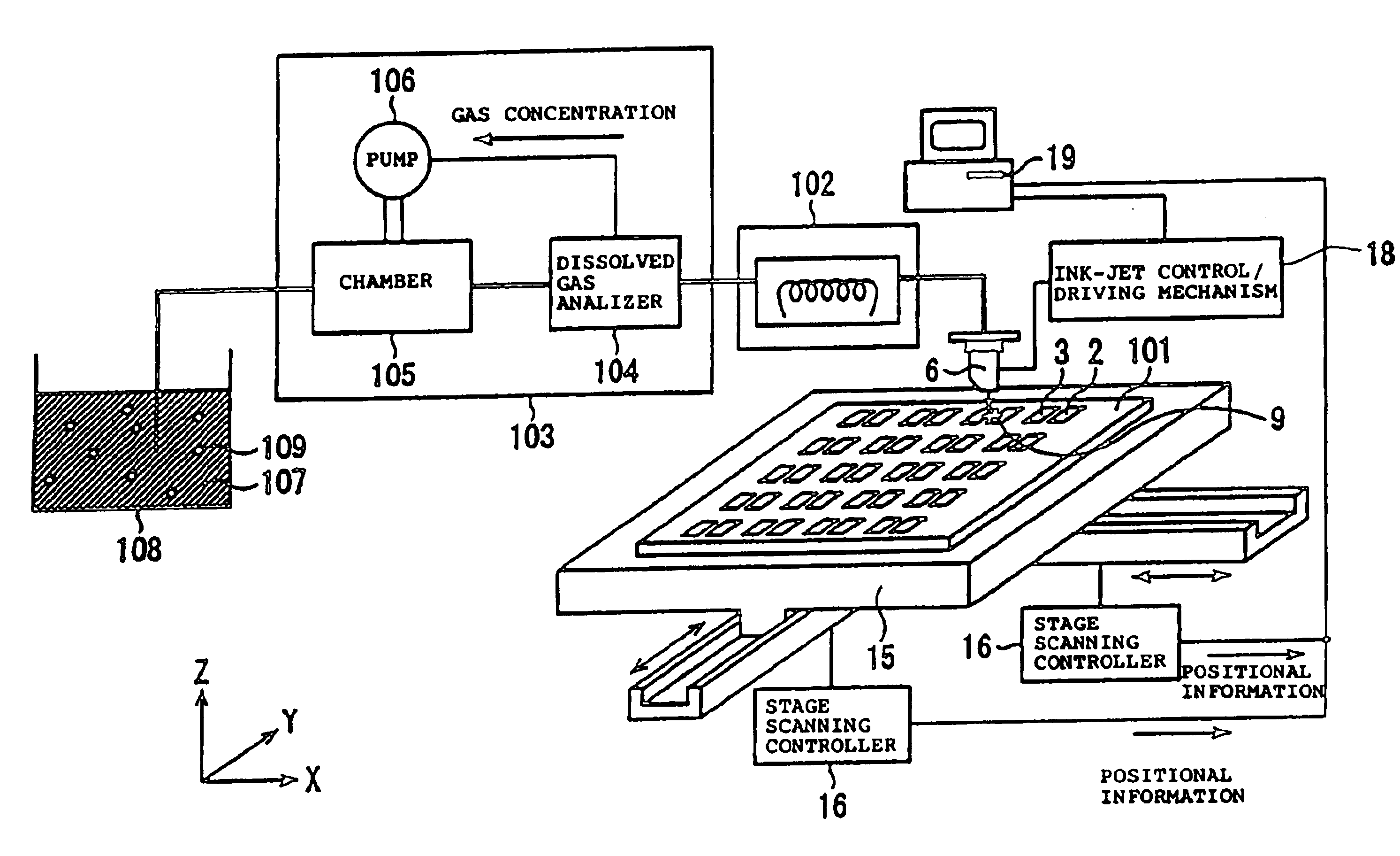
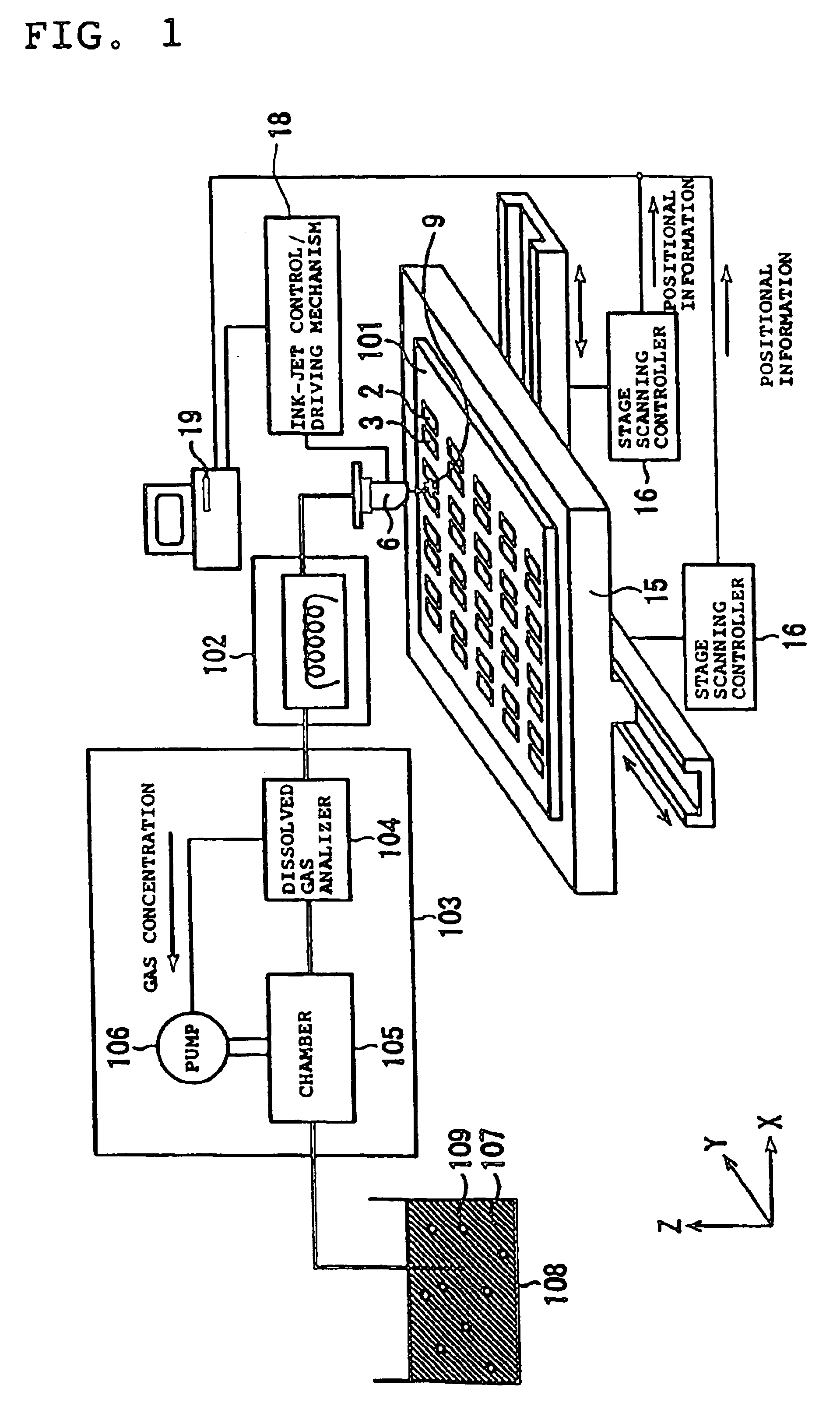
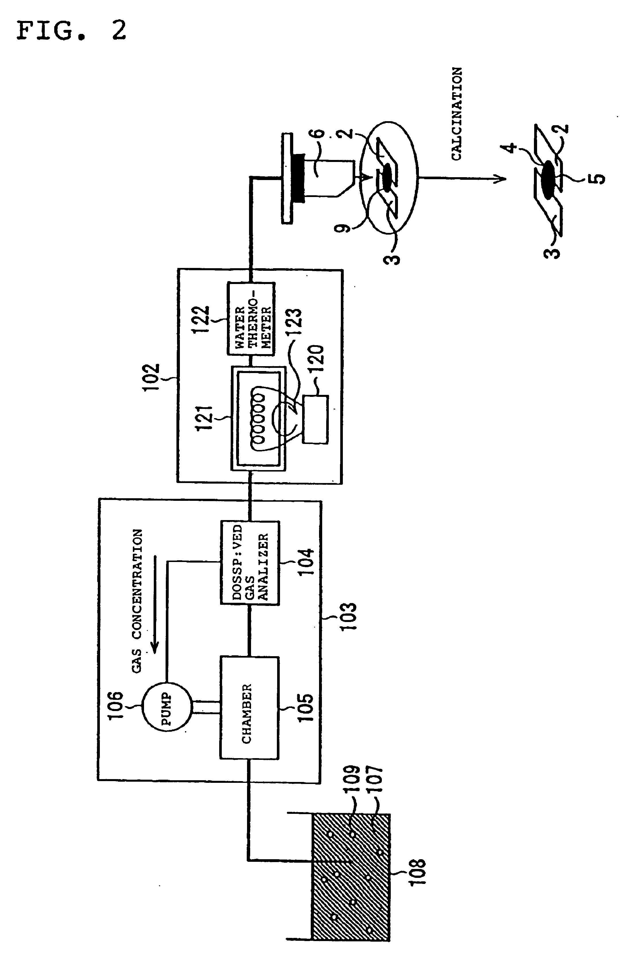
[0101]FIG. 1 is a view best showing the feature of the present invention, and shows an apparatus for forming the conductive film of a surface-conduction type electron-emitting element on an electron source substrate according to the present invention. FIG. 1 is a schematic view showing an electron source substrate manufacturing apparatus according to the first embodiment of the present invention. FIG. 2 is an enlarged view showing a system for supplying a metal solution to a droplet applying unit in FIG. 1. FIG. 3 is a view showing in detail a unit for removing a dissolved gas in FIG. 1.

[0102]The arrangement of this apparatus, and an electron source substrate manufacturing method using this apparatus will be explained. In FIG. 1, reference numeral 15 denotes a stage to which an MTX substrate 101 is fixed. The stage 15 is coupled to X- and Y-direction scanning mechanisms for moving the stage 15 in the X and Y directions, and can be moved to an arbitrary position in ...

second embodiment

(Second Embodiment)

[0125]A method of manufacturing an image forming apparatus having a surface-conduction type electron-emitting element according to the second embodiment of the present invention will be described with reference to FIG. 5. The second embodiment is the same as the first embodiment except that the concentration of a gas dissolved in a metal solution 107 is controlled by the opening degree of a valve 117.

[0126]When the exhaust speed of a vacuum pump 106 is set constant, the concentration of the gas dissolved in the metal solution 107 depends on the stay time in a chamber 105. In the second embodiment, the three-way valve 117 is interposed between the chamber 105 and a dissolved gas analyzer 104. The opening degree of the three-way valve 117 is controlled based on a dissolved O2 concentration detected by a DO meter 113, and part of the metal solution 107 is exhausted to the outside. This changes the stay time in the chamber 105 so as to keep the concentration of the ga...

third embodiment

(Third Embodiment)

[0128]A method of manufacturing an image forming apparatus having a surface-conduction type electron-emitting element according to the third embodiment of the present invention will be described with reference to FIG. 6. The third embodiment is the same as the first embodiment except that the concentration of a gas dissolved in a metal solution 107 is controlled by a pressure value in a chamber 105.

[0129]When discharge of droplets 9 from a droplet discharge unit 6 is maintained at a predetermined speed in manufacturing an electron source substrate, the stay time of the metal solution 107 in the chamber 105 is constant. At this time, the concentration of the gas dissolved in the metal solution 107 depends on the vacuum degree in the chamber 105. From this, as shown in FIG. 6, a pressure gauge 119 is arranged in the chamber 105. A pump control unit 110 is controlled based on the value of the pressure gauge 119 to keep the vacuum degree in the chamber 105 at a proper ...


PUM

PropertyMeasurementUnit
Temperatureaaaaaaaaaa
Concentrationaaaaaaaaaa

Abstract

An electron-emitting device manufacturing method comprising a gas removal step of removing a gas dissolved in a liquid containing a formation material of an electroconductive film in which an electron emitting area is to be formed, a temperature adjusting step of adjusting a temperature of the liquid from which the gas is removed, and a droplet discharge step of discharging droplets of which the temperature is adjusted by droplet discharge means in an ink jet manner, while controlling relative positions of the droplet discharge means and a substrate on which the electroconductive film in which the electron-emitting area is to be formed is formed. The droplets are thereby applied to a predetermined position on the substrate.

Description

[0001]This application is a continuation of International Application No. PCT / JP00 / 01024, filed Feb. 23, 2000, which claims the benefit of Japanese Patent Application No. 11-047095, filed Feb. 24, 1999.TECHNICAL FIELD[0002]The present invention relates to an electronic device manufacturing method and a manufacturing apparatus therefor and, more particularly, to a manufacturing method for an electronic device by the step of applying, to a substrate, droplets of a liquid containing the formation material of a member which constitutes the electronic device, and a manufacturing apparatus therefor.BACKGROUND ART[0003]As a method of easily manufacturing a surface-conduction type electron-emitting element at low cost, there is conventionally proposed a method like the one disclosed in Japanese Laid-Open Patent Application No. 8-171850 in which droplets of a metal-containing solution are discharged onto a substrate using a droplet discharge unit to form element electrodes and a conductive f...

Claims


Application Information

Patent Timeline
IPC IPC(8): B05D5/12B41J2/05C23C16/06H05K3/10B05C5/00B05C13/02H01J9/02B41J2/175B41J2/19
CPCB41J2/175B41J2/19H01J9/027B41J2/2107Y10T29/49155
Inventor MISHIMA, SEIJI
Owner CANON KK
Why Eureka
Try Eureka