Bump bonding method apparatus

a technology of pump and bonding method, applied in the direction of soldering apparatus, manufacturing tools,auxillary welding devices, etc., can solve the problem of difficult to achieve stable operation conditions that can be applied in practical industrial use, and achieve the effect of high reliability

Inactive Publication Date: 2005-06-07
PANASONIC CORP
View PDF24 Cites 15 Cited by
  • Summary
  • Abstract
  • Description
  • Claims
  • Application Information

AI Technical Summary

Benefits of technology

[0014]The present invention is devised in light of the foregoing conventional problems, and has an object to provide a bump bonding method and apparatus capable of joining a ball to a pad portion on an IC with high reliability without the need of heating from the outside, for example, using a heater, and also capable of forming a bump in a satisfactory joint condition.

Problems solved by technology

However, the reproducibility of the oscillation deteriorates at a frequency of 320 kHz or higher, which makes it difficult to achieve an operating condition stable enough to be applied to practical industrial use.

Method used


Image

  • Bump bonding method apparatus
  • Bump bonding method apparatus
  • Bump bonding method apparatus

Examples


Embodiment Construction

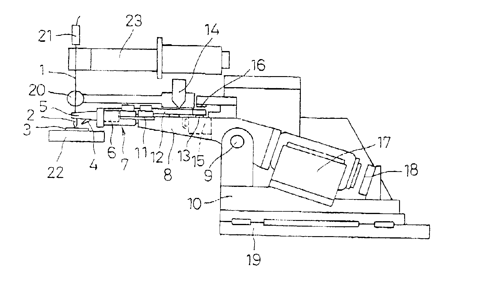
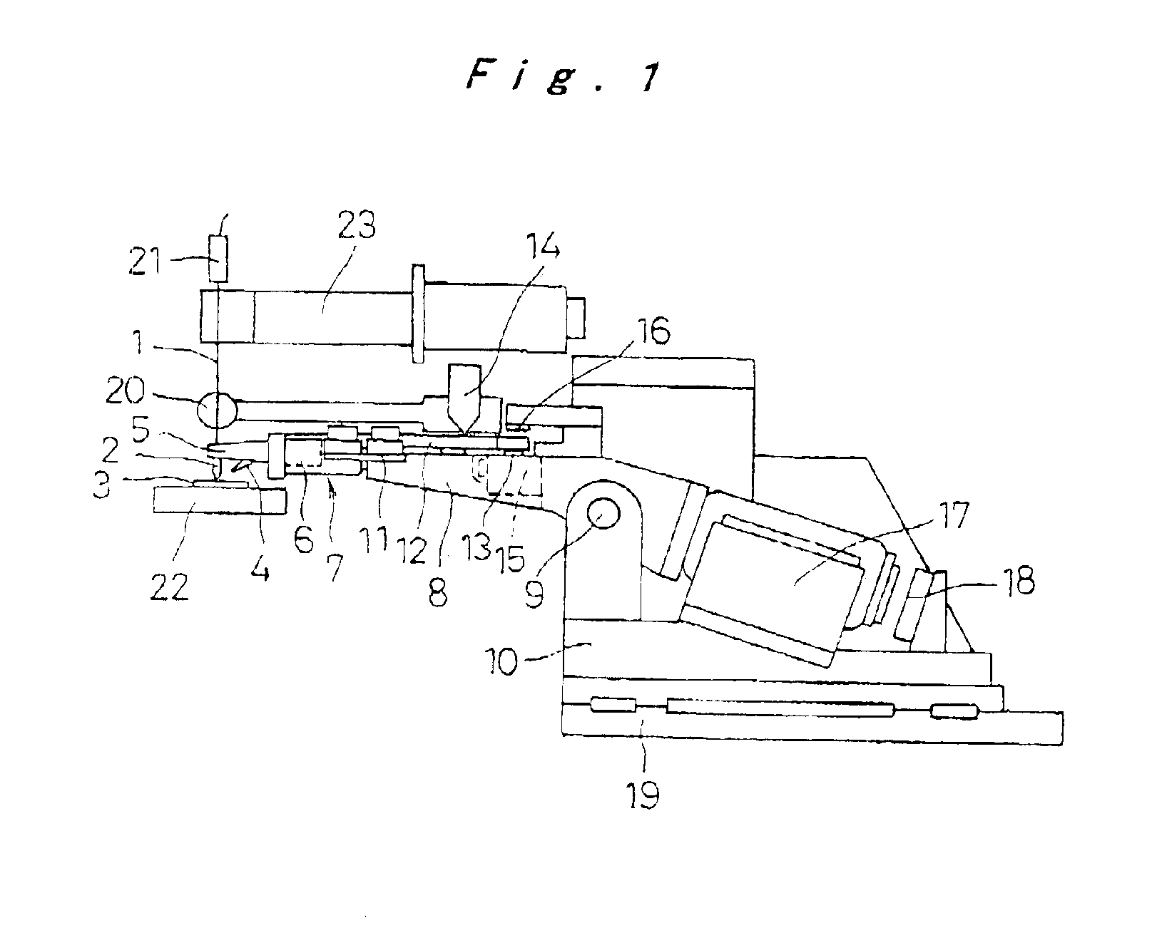
[0032]The following will describe one embodiment of a bump bonding apparatus of the invention with reference to FIG. 1 through FIG. 5.

[0033]Referring to FIG. 1, reference numeral 1 denotes a gold wire from which a ball is made, reference numeral 2 denotes a capillary through which the gold wire 1 penetrates, reference numeral 3 denotes an IC, reference numeral 4 denotes a discharge torch provided in close proximity to the tip of the gold wire 1, reference numeral 5 denotes a ultrasonic horn having the capillary 2 attached at the tip portion thereof, and reference numeral 6 denotes a ultrasonic transducer attached to the base portion of the ultrasonic horn 5. The capillary 2, the ultrasonic horn 5, and the ultrasonic transducer 6 together form an ultrasonic head 7. The ultrasonic transducer 6 is designed to have the resonant frequency of 230 kHz, and the ultrasonic horn 5 is designed to have a horn length as long as one wavelength of the ultrasonic vibration wavelength to reduce both...


PUM

PropertyMeasurementUnit
frequencyaaaaaaaaaa
frequencyaaaaaaaaaa
frequencyaaaaaaaaaa

Abstract

In a bump bonding technique for forming a bump on an IC, including forming a ball at the tip of a gold wire protruding from a capillary, and providing a metal-to-metal joint by applying ultrasonic vibration from a ultrasonic head through the capillary while pressing the ball against a pad portion on the IC, the metal-to-metal joint is provided by applying the ultrasonic vibration at a frequency in a range of 130 to 320 kHz, more preferably in a range of 170 to 270 kHz, and most preferably at a frequency of 230±10 kHz at room temperatures and atmospheric pressure. Consequently, a bump is formed on an IC having a low heat resistance temperature in a satisfactory joint condition, and a bump is formed with good positional accuracy without giving the influence of heat to the surroundings.

Description

[0001]The present disclosure relates to subject matter contained in priority Japanese Patent Application No. 2001-351874, filed on Nov. 16, 2001, the contents of which is herein expressly incorporated by reference in its entirety.BACKGROUND OF THE INVENTION[0002]1. Field of the Invention[0003]The present invention relates to a bump bonding method and apparatus used when fabricating a flip-chip semiconductor integrated circuit (hereinafter, referred to as an IC), for forming a protruding electrode (hereinafter, referred to as a stud bump or simply as a bump) on the IC.[0004]2. Description of Related Art[0005]Conventionally, a bump bonding technique is known which applies the wire bonding technique to form a bump. The bump is formed by the ultrasonic joining of a ball, made of gold or gold-plated metal, to an electrode pad (hereinafter, referred to simply as a pad) on the flip-chip IC.[0006]FIG. 7A and FIG. 7B show a typical embodiment of a conventional bump bonding apparatus. Referri...

Claims


Application Information

Patent Timeline
Patent Type & Authority Patents(United States)
IPC IPC(8): B23K20/00H01L21/60H01L21/607
CPCB23K20/007H01L24/11H01L2224/45015H01L24/12H01L24/45H01L2224/1134H01L2224/13144H01L2224/45144H01L2224/78301H01L2224/85045H01L2224/85205H01L2924/01002H01L2924/01004H01L2924/01013H01L2924/01025H01L2924/01039H01L2924/01079H01L2924/01082H01L2924/14H01L2924/20306H01L2924/20307H01L2924/20308H01L2924/20309H01L2924/00014H01L2924/01033H01L2924/01006H01L2924/01005H01L2924/00013H01L2224/13099H01L2924/00H01L2224/48H01L2924/20752H01L24/05H01L24/13H01L2224/05568H01L2224/05571H01L2224/05573H01L2224/05624H01L21/60
Inventor HORIE, SATOSHIYONEZAWA, TAKAHIROKIYOMURA, HIROYUKITOKUNAGA, TETSUYASASAOKA, TATSUO
Owner PANASONIC CORP
Why Eureka
Try Eureka