Atomic layer deposition systems and methods

a technology of atomic layer and deposition system, which is applied in the direction of polycrystalline material growth, crystal growth process, chemically reactive gas growth, etc., can solve the problems of limiting the throughput of the typical ald approach, limiting the total cycle to a typical time of approximately seven seconds, and a number of limitations

Inactive Publication Date: 2005-06-07
NOVELLUS SYSTEMS
View PDF16 Cites 86 Cited by
  • Summary
  • Abstract
  • Description
  • Claims
  • Application Information

AI Technical Summary

Benefits of technology

[0016]Atomic layer deposition systems and methods are disclosed herein. In accordance with one embodiment, rotary gas switching is provided for the ALD process within a multi-wafer sequential processing chamber. In accordance with another embodiment, ALD and conventional CVD are performed concurrently within a multi-wafer sequential processing chamber. The systems and methods disclosed herein allow the ALD process to be implemented in high-volume manufacturing applications.

Problems solved by technology

The typical ALD approach may be sufficient for research and development or low-volume production, but has a number of limitations.
For example, the throughput of the typical ALD approach is limited.
The limitations of gas switching technology, as well as the time required to purge the single wafer showerhead and reactor, limit the total cycle to a typical time of approximately seven seconds.
This limits the overall throughput of the CVD module or reactor to approximately 20 wafers per hour, which is unacceptable for most production requirements.
Single wafer processing chambers also have a significantly higher wafer transport and scheduling overhead as substrates must be moved to several modules.
Another drawback of single wafer systems is that in order to achieve the highest levels of throughput, the gas flow upstream of the throttle valve must be kept constant.
Constant flows are necessary because the cycle times are too short for a typical throttle valve pressure control system to adequately respond.
Additional drawbacks of single wafer reactors include cost and repeatability issues.
For example, the relatively complex manifold design inherent to single wafer systems leads to a high system cost.
Additionally, each single wafer system consumes a position on a high-vacuum wafer transfer system.
If the wafer transfer system is fully populated with single wafer systems to provide adequate throughput, a sufficient number of slots may not be available for other tasks.
This can lead to longer process startup and qualification times.

Method used


Image

  • Atomic layer deposition systems and methods
  • Atomic layer deposition systems and methods
  • Atomic layer deposition systems and methods

Examples


Embodiment Construction

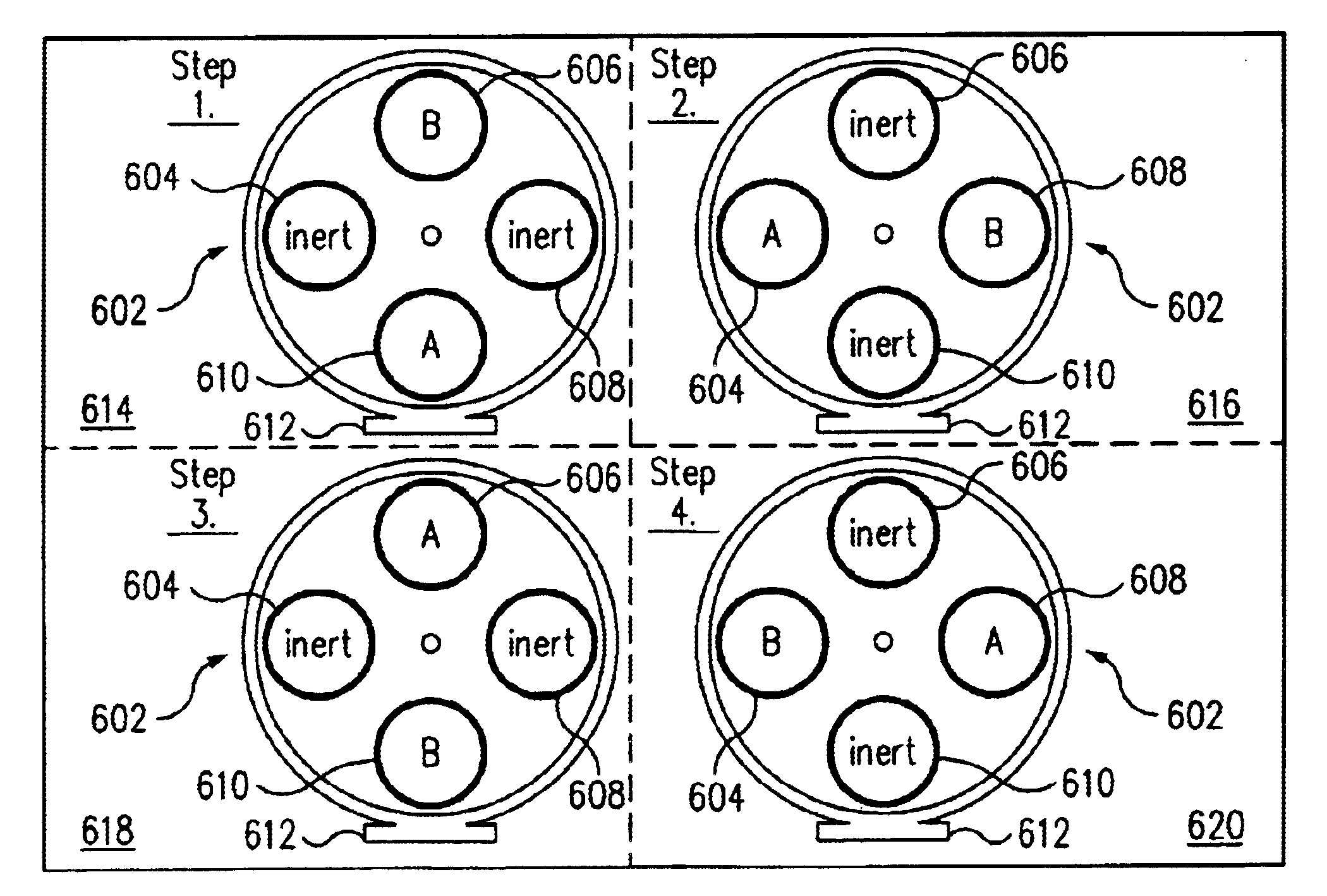
[0035]FIG. 5 shows a multi-wafer sequential deposition module 502 in accordance with an embodiment of the present invention. Multi-wafer sequential deposition module 502 includes five stations 504, 506, 508, 510, and 512 that are used to process wafers (e.g., such as wafer 516). Note that the number of stations provided by multi-wafer sequential deposition module 502 could vary depending upon the user's requirements. Stations 504 through 512 are each equipped with a wafer heater and a showerhead (which are not shown) and are optionally isolated from each other through the use of a continuous inert gas purge between, and independent pumping around, each station. An example of a multi-wafer sequential deposition module 502 is the Concept Three system by Novellus Systems (San Jose, Calif.).

[0036]Multiple wafers are processed sequentially and concurrently, receiving a portion of their total deposition thickness at each station. As an example, a wafer, such as wafer 516, enters multi-waf...


PUM

PropertyMeasurementUnit
timeaaaaaaaaaa
thicknessaaaaaaaaaa
electrical poweraaaaaaaaaa

Abstract

Atomic layer deposition systems and methods are disclosed utilizing a multi-wafer sequential processing chamber. The process gases are sequentially rotated among the wafer stations to deposit a portion of a total deposition thickness on each wafer at each station. A rapid rotary switching of the process gases eliminates having to divert the process gases to a system vent and provides for atomic layer film growth sufficient for high-volume production applications. Conventional chemical vapor deposition can also be performed concurrently with atomic layer deposition within the multi-wafer sequential processing chamber.

Description

BACKGROUND OF THE INVENTION[0001]1. Field of the Invention[0002]The present invention relates generally to semiconductor processing and, more particularly, to chemical vapor deposition.[0003]2. Related Art[0004]Atomic layer deposition (ALD), also known as atomic layer chemical vapor deposition (ALCVD), is a method for producing very thin films that are highly conformal, smooth, and possess excellent physical properties. ALD uses volatile gases, solids, or vapors that are sequentially introduced (or pulsed) over a heated substrate. A first precursor is introduced as a gas, which is absorbed (or adsorbed) into the substrate and the reactor chamber is cleared of the gaseous precursor. A second precursor is introduced as a gas, which reacts with the absorbed precursor to form a monolayer of the desired material. By regulating this sequence, the films produced by ALD are deposited a monolayer at a time by repeatedly switching the sequential flow of two or more reactive gases over the sub...

Claims


Application Information

Patent Timeline
Patent Type & Authority Patents(United States)
IPC IPC(8): C30B25/00C30B23/00C23C16/455C23C16/54C30B25/02C30B25/14H01L21/00H01L21/687
CPCC23C16/45551C23C16/45565C23C16/54C30B25/02H01L21/68771H01L21/6719H01L21/67207H01L21/68764C30B25/14
Inventor OMSTEAD, THOMAS R.LEVY, KARL B.
Owner NOVELLUS SYSTEMS
Why Eureka
Try Eureka