Manufacturing methods for printed circuit boards

a manufacturing method and printed circuit board technology, applied in the field of printed circuit board manufacturing methods, can solve the problems of poor electrical characteristics of polyimides, standard methods used to form bumps on printed circuit boards that cannot meet these requirements, and roll processing is not suitable for teflon-based materials, etc., to achieve the effect of increasing the rigidity of a multi-layer structure and being easy to handl

Inactive Publication Date: 2005-06-07
GLOBALFOUNDRIES INC
View PDF9 Cites 151 Cited by
  • Summary
  • Abstract
  • Description
  • Claims
  • Application Information

AI Technical Summary

Benefits of technology

[0013]The present invention is also related to a method for increasing the rigidity of a multi-layer structure that is used to form a flexible printed circuit board. The method comprises the steps of applying a metal layer having a first height on at least one surface of a dielectric substrate; applying a first photoresist to the metal layer, imaging the photoresist to provide at least one section of remaining photoresist defining an opening therein and at least one exposed region of the metal layer; etching the exposed region of the metal layer to a second height; and removing the remaining photoresist to provide a multi-layered structure comprising a dielectric layer and a metal layer comprising at least one region having a second height and at least one region having a first height. The region having the second height is the basis for the electrical circuitry that is formed during subsequent manufacturing steps. Preferably, the region having the first height, hereinafter referred to as a “border”, surrounds the region having the second height. The border reinforces the multi-layer structure during subsequent manufacturing steps, thus rendering the multi-layer structure easier to handle.

Problems solved by technology

Unfortunately, the standard methods that are used to form bumps on a printed circuit board do not easily meet these requirements.
Although roll processing is suitable for materials that have good mechanical strength and tear resistance, such as polyimides, roll processing is not suitable for Teflon-based materials, which typically have better electrical characteristics than polyimides but poorer mechanical properties.
Roll processing is also not suitable for the manufacture of the very thin, low dielectric polymers that typically lack the continuous glass fiber reinforcement of rigid printed circuit boards.
Furthermore, roll processing is not readily adaptable to fabricating cables with multiple conductive layers where lamination of additional dielectric layers would be required.
During processing, the circuit board is subjected to stretching which can cause damage, such as tearing or wrinkling of the thin panel.
Furthermore, the panels tend to shrink or grow as they go through various thermal excursions, or etching, or plating of copper, or addition of dielectric layers.
Since the final product has precise dimensional requirements and requires precise layer to layer alignment, this change in size is problematic.
Accordingly, special steps must be taken to prevent damage of flexible cables during fabrication which often offsets the performance advantages of these products with large cost penalties.
Thus, panel processing is not well suited to the fabrication of thin flexible cables or thin circuit boards.
Since each hole must be drilled individually, this process is time-consuming and expensive.
Nonetheless, the blind vial can be very difficult to clean and plate because process fluids cannot flow through the smaller hole.
As a result, the process fluids tend to get trapped in the vias.
The accumulation of flux and solder in the vias ultimately can lead to failure of the resulting printed circuit board.
However, such hole filling methods tend to add additional processing and material costs to the fabrication of a printed circuit board.

Method used


Image

  • Manufacturing methods for printed circuit boards
  • Manufacturing methods for printed circuit boards
  • Manufacturing methods for printed circuit boards

Examples


Embodiment Construction

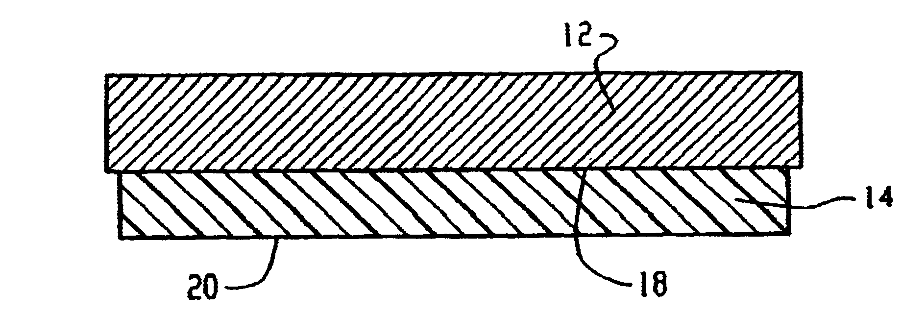
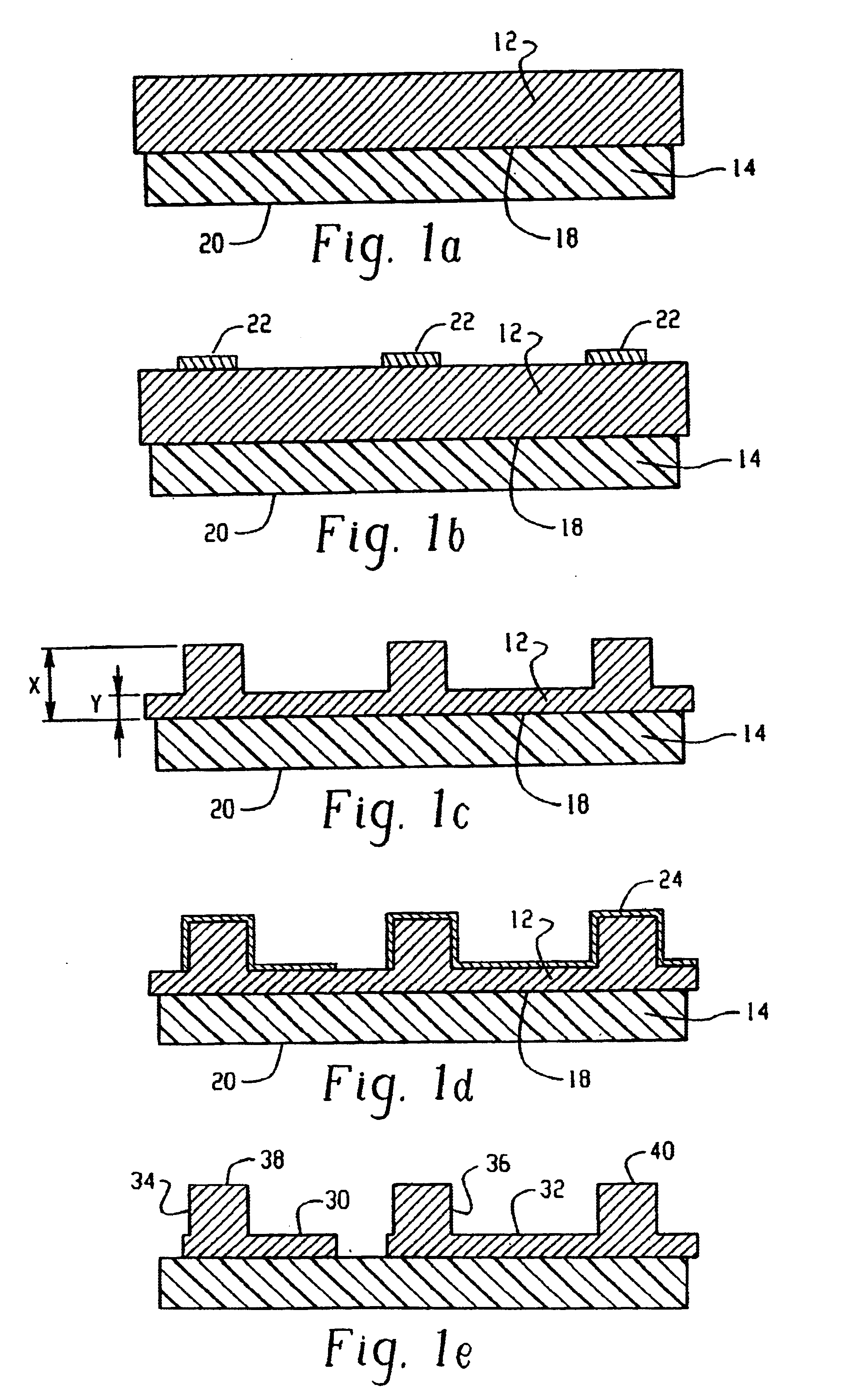
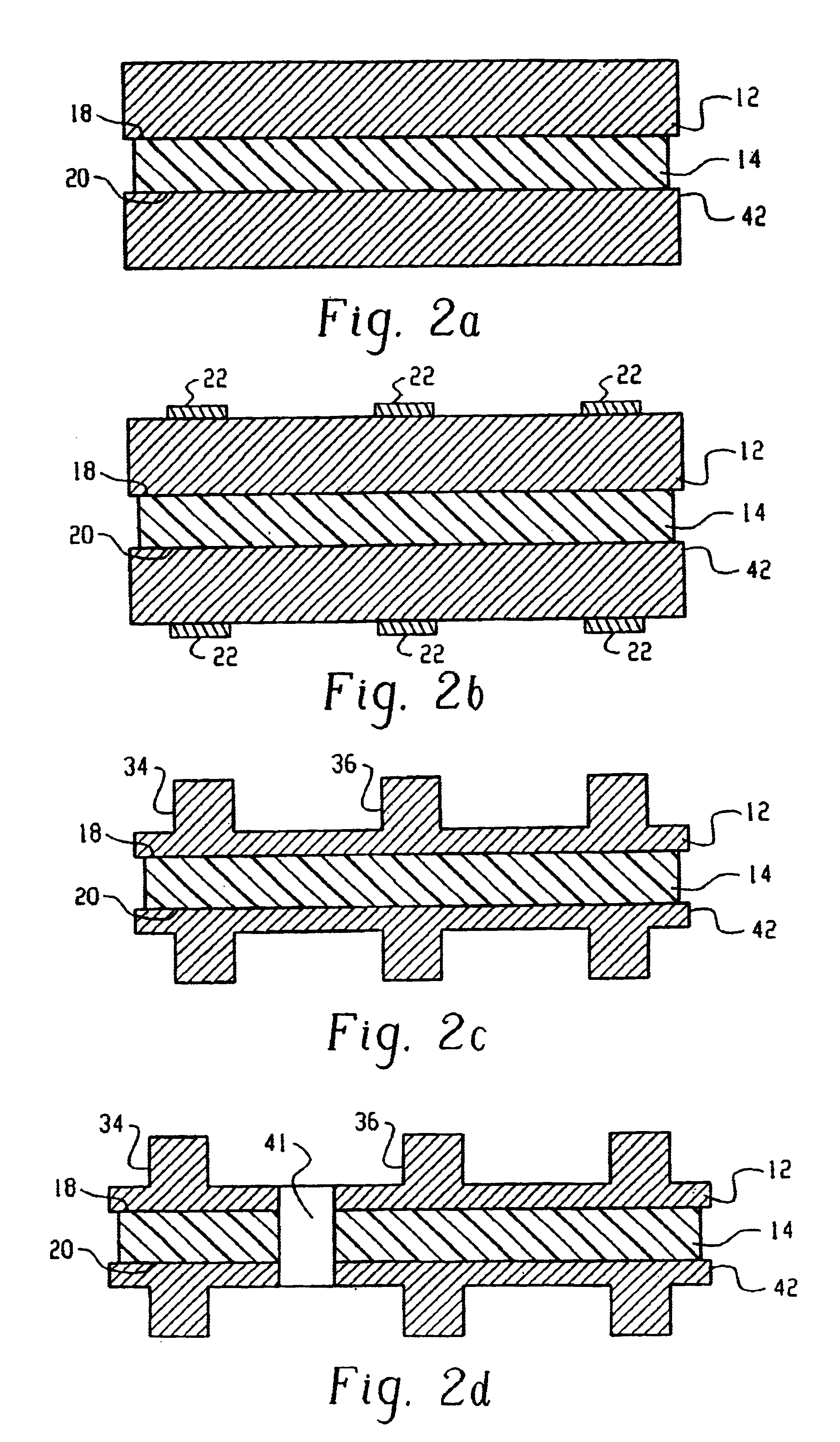
[0020]In accordance with the present invention, a conductive layer comprising a plurality of conductive bumps, a plurality of electrically conductive circuit lines, and a plurality of contact pads is subtractively formed from a single substantially planar layer of metal that has been disposed on a surface of a dielectric layer. Because the lines, pads and bumps are all formed from a single metallic layer, the bumps, pads, and lines are electrically connected and continuous. As used herein the term “continuous” means that there are no interfaces between the conductive bumps, the contact pads, and the circuit lines. In one embodiment, a first metal layer, preferably a substantially planar metal layer, having a first height (x) is disposed on at least one surface of the dielectric substrate through plating or, preferably, through lamination of a metal foil to the substrate. A first photoresist is then applied to the exposed surface of the first metal layer. The first photoresist is ima...


PUM

PropertyMeasurementUnit
sizeaaaaaaaaaa
diameteraaaaaaaaaa
diameteraaaaaaaaaa

Abstract

A method of forming a plurality of solid conductive bumps for interconnecting two conductive layers of a circuit board with substantially coplanar upper surfaces. The method comprises the steps of applying a continuous homogenous metal layer onto a dielectric substrate, applying a first photoresist and exposing and developing said first photoresist to define a pattern of conductive bumps; etching the metal layer exposed by said development to form said plurality of conductive bumps; removing said first photoresist; applying a second photoresist onto the metal layer; exposing and developing said second photoresist to define a pattern of conductive bumps and circuit lines; etching the metal layer exposed by said development to form a pattern of circuit lines in said metal layer; and removing said second photoresist. The methods of the present invention also provides for fabricating a multilayer circuit board and a metallic border for providing rigidity to a panel.

Description

CROSS-REFERENCE TO RELATED APPLICATIONS[0001]This application is a division of application Ser. No. 09 / 789,156, filed Feb. 20, 2001, now U.S. Pat. No. 6,684,497 which in turn is a division of Ser. No. 08 / 968,988 filed on Nov. 12, 1997 now U.S. Pat. No. 6,222,136 B1.FIELD OF THE INVENTION[0002]This invention relates to methods of manufacturing printed circuit boards, particularly printed circuit boards having substantially coplanar conductive bumps on the surface thereof and to printed circuit boards having solid interconnects between the conductive layers thereof.BACKGROUND OF THE INVENTION[0003]Standard flexible printed circuit boards comprise a flexible dielectric substrate having circuit lines attached to one or more surfaces thereof. Typically, electrical connections are made between such printed circuit boards and other electrically conductive components by means of conductive bumps which are in electrical communication with the circuit lines. Usually, the conductive bumps are ...

Claims


Application Information

Patent Timeline
Patent Type & Authority Patents(United States)
IPC IPC(8): H05K3/40H05K3/06H05K3/46H05K3/20H05K3/42
CPCH05K3/06H05K3/4007H05K3/4647Y10T29/49146H05K3/427H05K3/4614H05K3/4617H05K2201/0367H05K2201/09563H05K2201/09736H05K2203/0369H05K2203/0733H05K2203/1572Y10T29/49156Y10T29/49165Y10T29/49002Y10T29/49117Y10T29/49128Y10T29/49155Y10T29/49126H05K3/20H05K3/00
Inventor APPELT, BERND KARL-HEINZBUPP, JAMES RUSSELLFARQUHAR, DONALD SETONKEESLER, ROSS WILLIAMKLODOWSKI, MICHAEL JOSEPHSEMAN, ANDREW MICHAELSCHILD, GARY LEE
Owner GLOBALFOUNDRIES INC
Why Eureka
Try Eureka