Strained silicon structure

a technology of strained silicon and crystalline silicon, applied in the direction of transistors, semiconductor devices, electrical equipment, etc., can solve the problems of significant challenges, high defect density may present a significant barrier for the production of integrated circuits using such substrates, and relaxed crystalline silicon is said to be lattice-mismatched with respect to relaxed crystalline sig

Inactive Publication Date: 2005-06-07
TAIWAN SEMICON MFG CO LTD
View PDF50 Cites 85 Cited by
  • Summary
  • Abstract
  • Description
  • Claims
  • Application Information

AI Technical Summary

Benefits of technology

[0005]The problems and needs outlined above may be addressed by embodiments of the present invention. In accordance with one aspect of the present invention, a semiconductor device is provided, which includes a substrate, a first epitaxial layer, a second epitaxial layer, a third epitaxial layer, a first trench, and a second trench. The first epitaxial layer is formed on the substrate. The first layer has lattice mismatch relative to the substrate. The second epitaxial layer is formed on the first layer, and the second layer has lattice mismatch relative to the first layer. The third epitaxial layer is formed on the second layer, and the third layer has lattice mismatch relative to the second layer. The first trench extends through the first layer. The second trench extends through the third layer and at least partially through the second layer. At least part of the second trench is aligned with at least part of the first trench, and the second trench is at least partially filled with an insulating material.
[0006]In accordance with another aspect of the present invention, a method of manufacturing a semiconductor device, is provided. This method includes the following steps described in this paragraph, and the order of steps may vary. A substrate is provided. A first epitaxial layer is formed on the substrate. The first layer has lattice mismatch relative to the substrate. A first trench is formed in the first layer. A second epitaxial layer is formed on the first layer. The second layer has lattice mismatch relative to the first layer. A third epitaxial layer is formed on the second layer. The third layer has lattice mismatch relative to the second layer. A second trench is formed in the third and second layers. At least part of the second trench is in alignment with at least part of the first trench.
[0006]In accordance with another aspect of the present invention, a method of manufacturing a semiconductor device, is provided. This method includes the following steps described in this paragraph, and the order of steps may vary. A substrate is provided. A first epitaxial layer is formed on the substrate. The first layer has lattice mismatch relative to the substrate. A first trench is formed in the first layer. A second epitaxial layer is formed on the first layer. The second layer has lattice mismatch relative to the first layer. A third epitaxial layer is formed on the second layer. The third layer has lattice mismatch relative to the second layer. A second trench is formed in the third and second layers. At least part of the second trench is in alignment with at least part of the first trench.

Problems solved by technology

Significant challenges are faced when CMOS devices are scaled into the sub-100 nm regime.
Relaxed crystalline silicon is said to be lattice-mismatched with respect to relaxed crystalline SiGe due to the difference in their lattice constants.
Such a high defect density may present a significant barrier for the production of integrated circuits using such substrates.
Also, the underlying strain fields of the misfit arrays result in a characteristic cross-hatch surface roughness.
This surface roughness can be a significant problem as it potentially degrades channel mobility in active devices.

Method used


Image

  • Strained silicon structure
  • Strained silicon structure
  • Strained silicon structure

Examples


Embodiment Construction

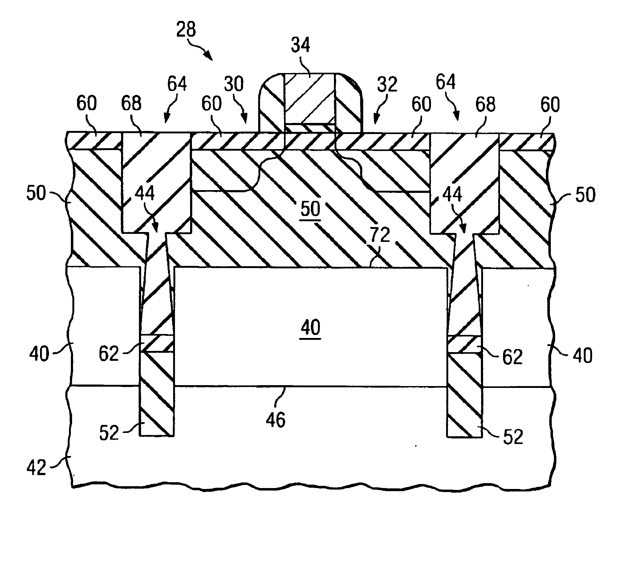
[0013]Referring now to the drawings, wherein like reference numbers are used herein to designate like elements throughout the various views, illustrative embodiments of the present invention are shown and described. The figures are not necessarily drawn to scale, and in some instances the drawings have been exaggerated and / or simplified in places for illustrative purposes only. One of ordinary skill in the art will appreciate the many possible applications and variations of the present invention based on the following illustrative embodiments of the present invention.

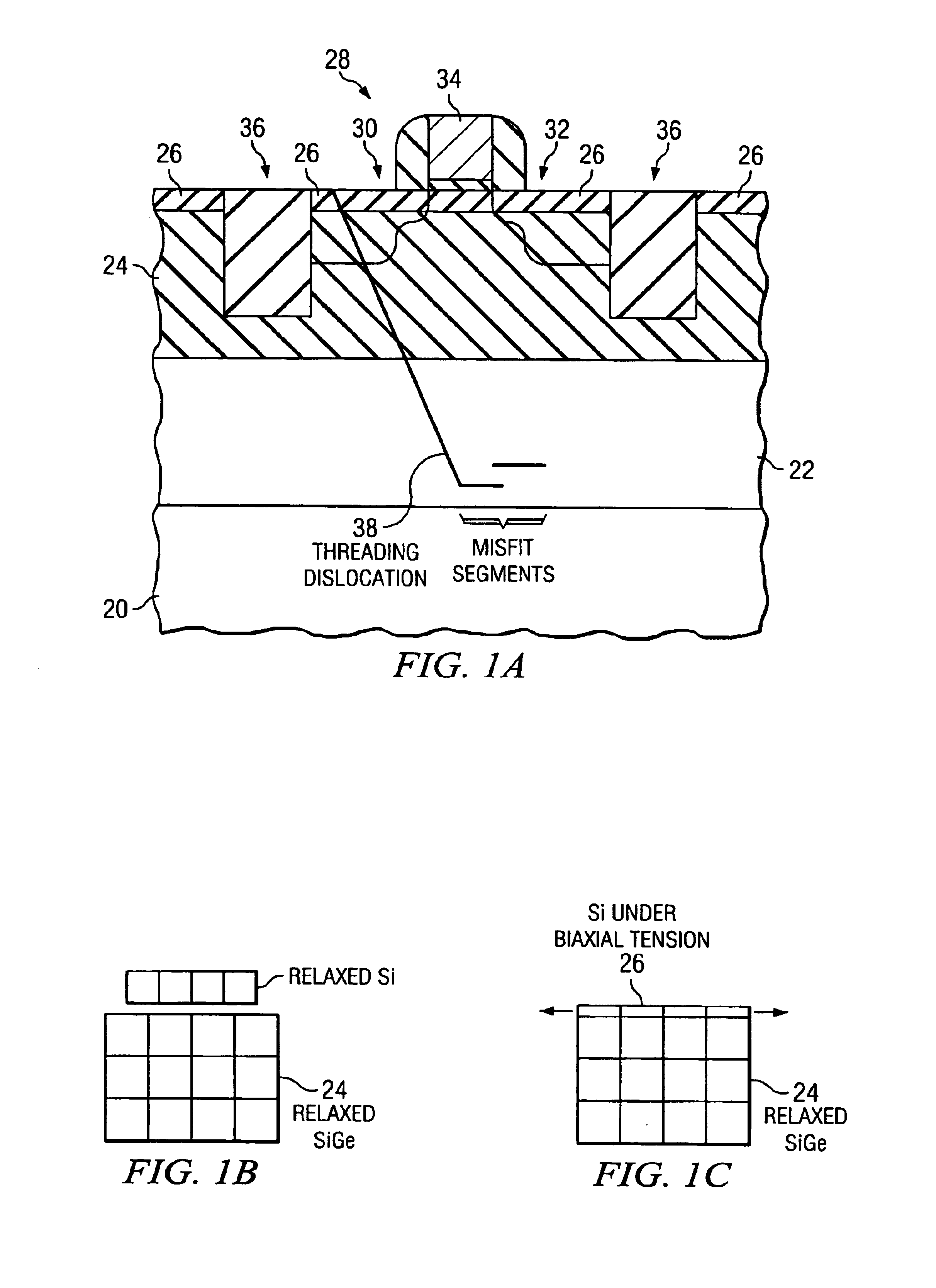
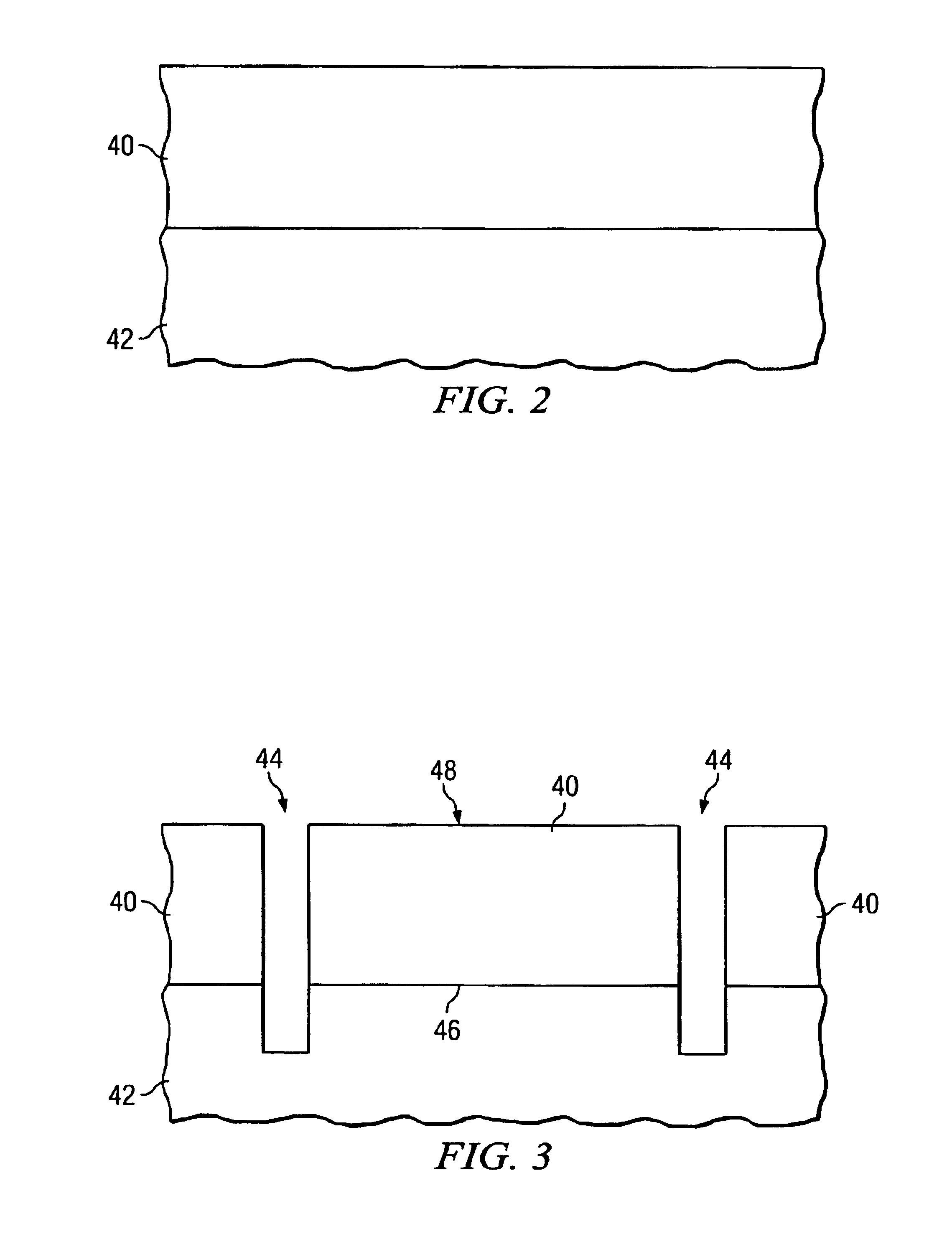
[0014]FIGS. 2-11 show process steps for two illustrative embodiments of the present invention. An embodiment of the present invention provides a way to reduce defect density in an improved strained silicon structure, as compared to the prior design (see FIG. 1A), for example. One of the primary mechanisms for achieving reduced defect density in an embodiment of the present invention is providing free surfaces for grain ...


PUM


Abstract

A semiconductor device includes a substrate, a first epitaxial layer, a second epitaxial layer, a third epitaxial layer, a first trench, and a second trench. The first epitaxial layer is formed on the substrate. The first layer has lattice mismatch relative to the substrate. The second epitaxial layer is formed on the first layer, and the second layer has lattice mismatch relative to the first layer. The third epitaxial layer is formed on the second layer, and the third layer has lattice mismatch relative to the second layer. Hence, the third layer may be strained silicon. The first trench extends through the first layer. The second trench extends through the third layer and at least partially through the second layer. At least part of the second trench is aligned with at lease part of the first trench, and the second trench is at least partially filled with an insulating material.

Description

TECHNICAL FIELD[0001]The present invention generally relates to the fabrication of semiconductor devices. In one aspect it relates more particularly to a strained silicon structure.BACKGROUND[0002]Complementary metal-oxide-semiconductor (CMOS) technology is a dominant semiconductor technology used for the manufacture of ultra-large scale integrated (ULSI) circuits today. Size reduction of the metal-oxide-semiconductor field-effect transistor (MOSFET) has provided significant improvement in the speed performance, circuit density, and cost per unit function of semiconductor chips over the past few decades. Significant challenges are faced when CMOS devices are scaled into the sub-100 nm regime. An attractive approach for additional improvement of CMOS transistor performance exploits strain-induced band-structure modification and mobility enhancement to increase the transistor drive current. Enhanced electron and hole mobilities in silicon (Si) under biaxial tensile strain can be achie...

Claims


Application Information

Patent Timeline
Patent Type & Authority Patents(United States)
IPC IPC(8): H01L21/762H01L21/336H01L21/20H01L21/02H01L29/74H01L29/78H01L21/70H01L21/338H01L29/66H01L31/072H01L31/0264H01L31/06H01L31/0328H01L21/8238H01L29/08H01L29/10
CPCH01L21/823807H01L21/823878H01L29/0847H01L29/7842H01L29/6659H01L29/7833H01L29/1054
Inventor GE, CHUNG-HULEE, WEN-CHINHU, CHENMING
Owner TAIWAN SEMICON MFG CO LTD
Why Eureka
Try Eureka