Ultra-high bandwidth multi-port memory system for image scaling applications

a multi-port memory and image scaling technology, applied in the field of memory systems, can solve the problems of large sram line memory devices occupying valuable and costly silicon area, increasing defect and failure potential, etc., and achieves the effects of improving silicon area usage, improving reliability, and reducing costs

Inactive Publication Date: 2005-06-07
PIXELWORKS
View PDF18 Cites 50 Cited by
  • Summary
  • Abstract
  • Description
  • Claims
  • Application Information

AI Technical Summary

Benefits of technology

[0012]The image scaling memory system of the present invention eliminates the use of internal or external line memories by using an existing frame memory coupled with an input buffer and a plurality of output buffers for providing a vertical scalar with simultaneous parallel access to m

Problems solved by technology

The separate SRAM and DRAM requirements increase design complexity, which necessarily increases defect and

Method used


Image

  • Ultra-high bandwidth multi-port memory system for image scaling applications
  • Ultra-high bandwidth multi-port memory system for image scaling applications
  • Ultra-high bandwidth multi-port memory system for image scaling applications

Examples


Embodiment Construction

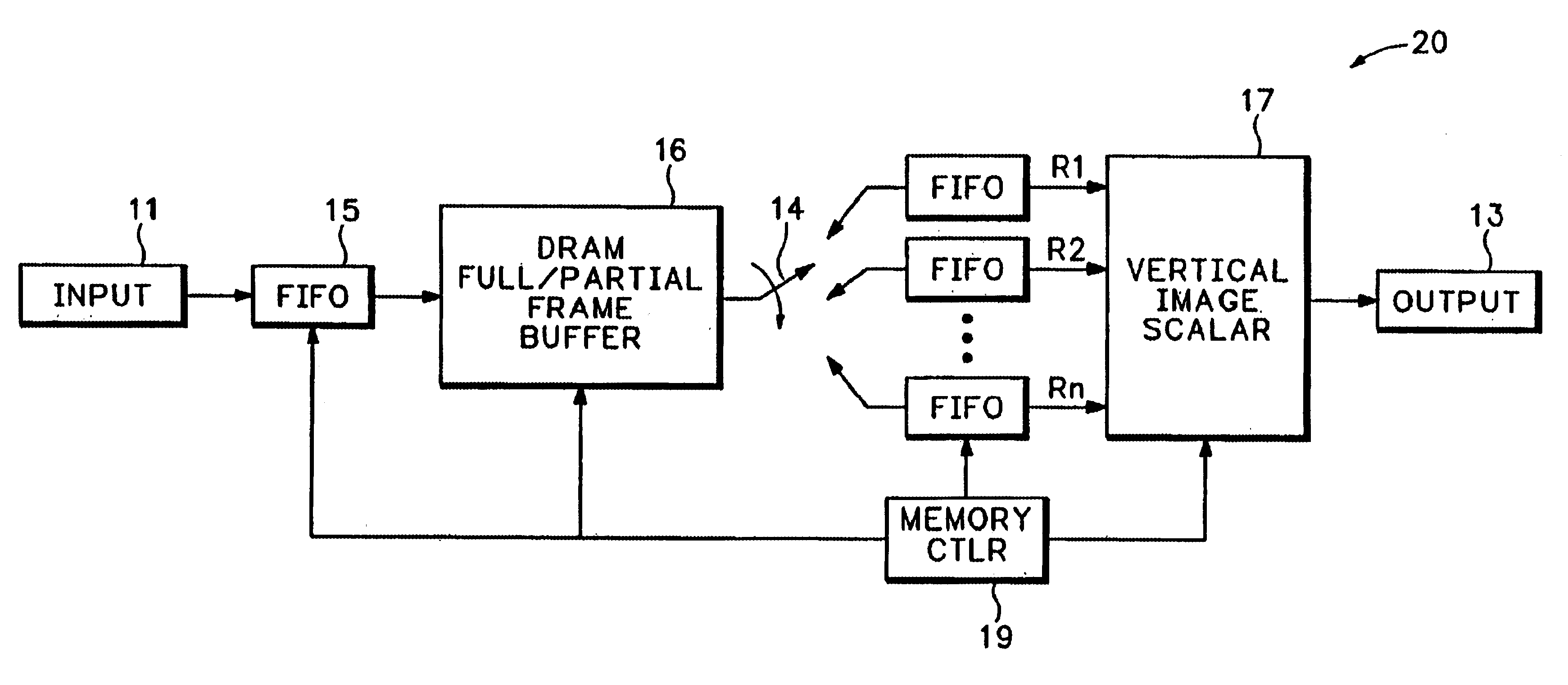
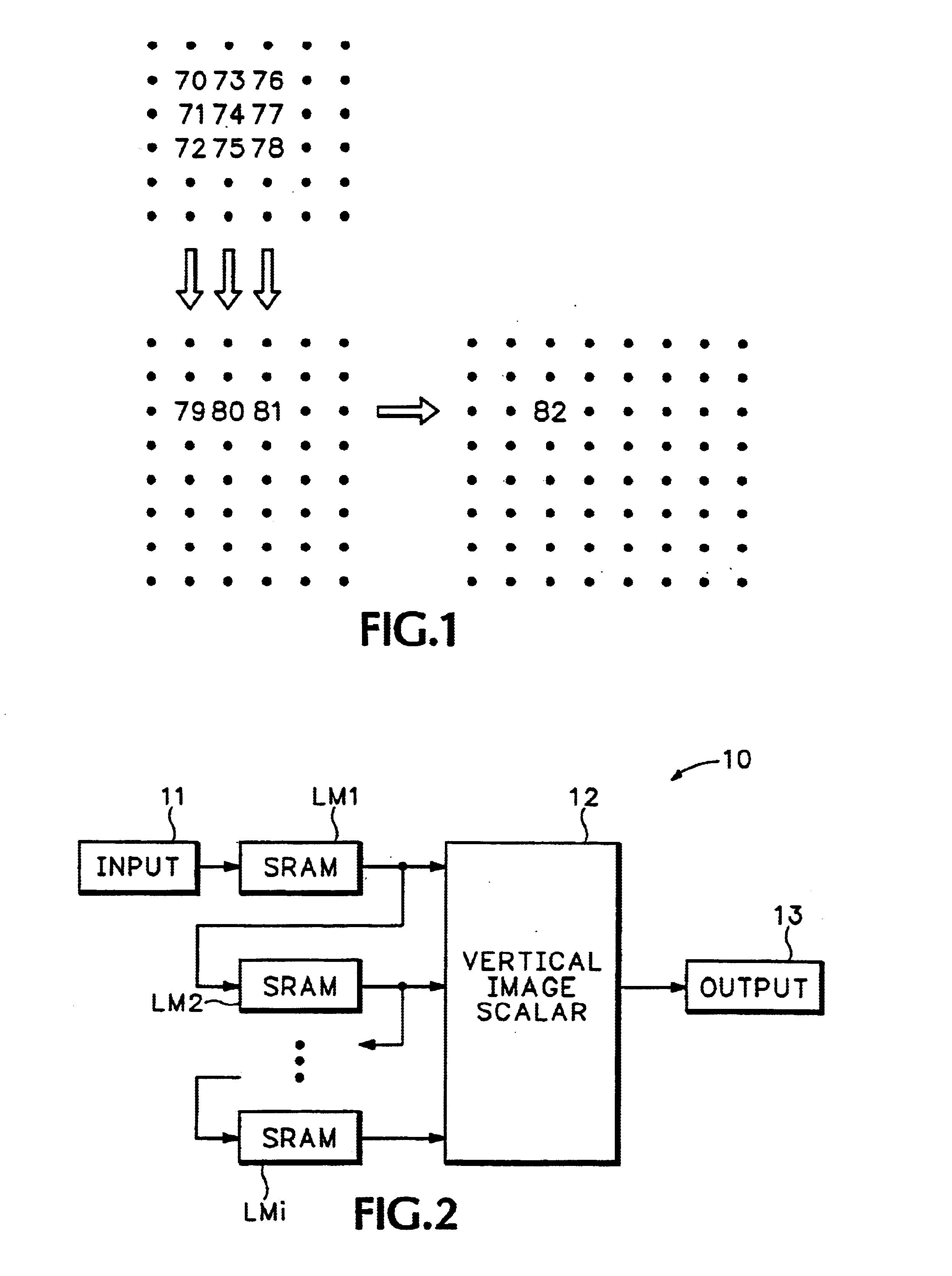
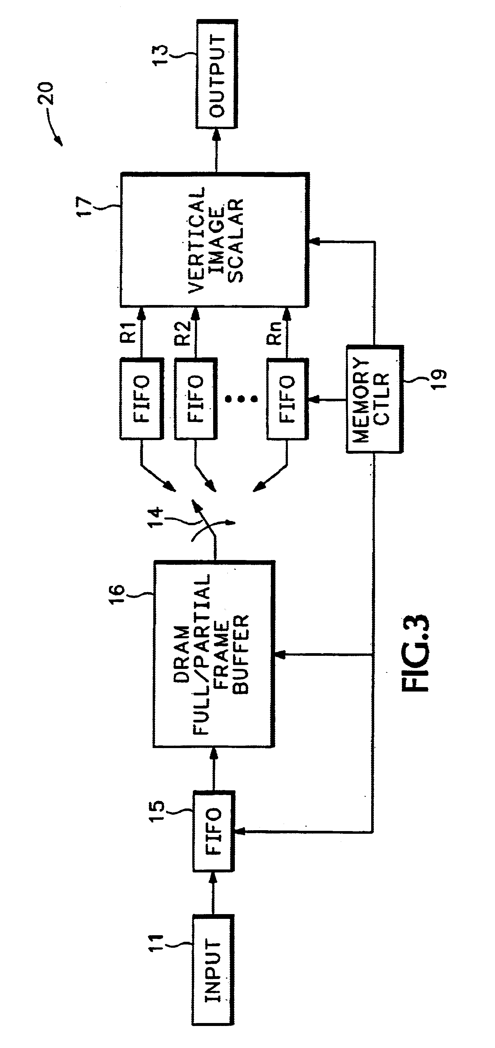
[0039]FIG. 3 is a block diagram of an image scaling circuit 20 of the present invention. At the heart of the image scaling circuit 20 is the multipurpose frame memory 16. The multipurpose frame memory 16 is coupled to an input buffer 15 at an input side and to a plurality of output buffers, like registers R1, R2, . . . Rn, at an output side. The plurality of output buffers R1, R2, . . . Rn are directly coupled to a vertical image scalar 17 for scaling the digital image data 11 in a vertical direction. The digital image data 11 is a stream of pixels representing an image to be scaled and ultimately displayed. The vertical image scalar 17 generates the digital output signal 13 by vertically scaling the buffered digital image data provided by the plurality of output buffers R1, R2, . . . Rn. Packet based transfer of the digital image data 11 is made possible by surrounding the frame memory 16 with small registers like input buffer 15 and the plurality of output buffers R1, R2, . . . Rn...


PUM


Abstract

The image scaling memory system of the present invention eliminates the use of internal or external line memories by using an existing frame memory coupled with an input buffer and a plurality of output buffers for providing a vertical scalar with simultaneous parallel access to multiple lines of data. Additionally, the image scaling memory system of the present invention, including the frame memory, is embedded into an integrated circuit. Thus, the image scaling circuit of the present invention improves reliability, lowers cost, and improves silicon area usage. The frame memory is coupled to an input buffer at an input side and a plurality of output buffers at an output side. The plurality of output buffers is positioned between the frame memory and the vertical scalar. Each output buffer sequentially gains access to and transfers portions of image lines from the frame buffer. Each output buffer stores only a portion of an image line resulting in relatively small output buffers. The plurality of output buffers provides the vertical scalar with simultaneous parallel access to multiple lines of buffered digital image data. The frame memory preferably comprises DRAM that stores the image data such that row faults are minimized. The DRAM frame memory preferably includes at least two memory banks, each including a plurality of rows and a plurality of columns. The DRAM frame memory has multiple purposes including storing digital image data frames for sample rate conversion, as well as, storing bitmaps for access by an On Screen Display controller and storing microprocessor data for access by a microprocessor.

Description

[0001]This application is a continuation of U.S. patent application Ser. No. 09 / 313,060, filed May 17, 1999, that claims priority from U.S. patent application No. Ser. 09 / 198,314, filed Nov. 23, 1998, U.S. Pat. No. 6,339,434 that claims priority from U.S. Provisional Patent Application No. 60 / 065,445, filed Nov. 24, 1997, and U.S. Provisional Patent Application No. 60 / 086,121, filed May 20, 1998, all incorporated herein by reference.BACKGROUND OF THE INVENTION[0002]1. Field of the Invention[0003]This invention relates to a memory system for the visual display of digital image data and, more particularly, to an embedded ultra-high bandwidth multi-port memory system for digital image scaling applications.[0004]2. Description of the Prior Art[0005]Digital image data generally defines one or more frames. A frame is an image displayed for viewing on a display or panel at one time, i.e., one frame of data fits on the display screen or panel. Each frame includes a rectangular array of pixe...

Claims


Application Information

Patent Timeline
IPC IPC(8): G09G5/395G09G5/391G06T3/40G09G5/36
CPCG06T3/4084G09G5/395G09G5/391G09G2340/0407
Inventor GREENBERG, ROBERT Y.WEST, MICHAEL G.
Owner PIXELWORKS
Why Eureka
Try Eureka