Liquid crystal display device with a counter voltage line intersecting the drain lines

a liquid crystal display and counter voltage technology, applied in the direction of identification means, instruments, optics, etc., can solve the problems of loss of initial function, corrosion of aluminum, ito or the like, etc., and achieve the effect of increasing the time constant of the display device, increasing the capacitance, and increasing the capacitan

Inactive Publication Date: 2005-06-07
PANASONIC LIQUID CRYSTAL DISPLAY CO LTD +1
View PDF1 Cites 42 Cited by
  • Summary
  • Abstract
  • Description
  • Claims
  • Application Information

AI Technical Summary

Benefits of technology

[0020]Since the transparent conductive films (ITO or the like) which constitute the gate line and the pixel are formed on the same plane of the insulative substrate, it is possible to increase the screen size of a liquid crystal display device having a high aperture ratio and a high viewing angle.
[0035]In addition, since an aluminum line is used, the occurrence of hillocks can be reduced by oxidizing the required portion of the aluminum line and the occurrence of a display defect such as a smear on the screen is prevented, whereby a highly reliable liquid crystal display device can be obtained.

Problems solved by technology

In addition, there are some cases where if a pattern of ITO or the like is formed after the formation of an aluminum pattern (interconnecting pattern), aluminum is corroded during the etching of ITO or the like and an initial function is lost.
In addition, if an interconnection line is formed of aluminum, it is difficult to electrically connect ITO or the like, which constitutes an oxide transparent conductive layer, with an aluminum film in the state of being in direct contact with the aluminum film.

Method used


Image

  • Liquid crystal display device with a counter voltage line intersecting the drain lines
  • Liquid crystal display device with a counter voltage line intersecting the drain lines
  • Liquid crystal display device with a counter voltage line intersecting the drain lines

Examples


first embodiment

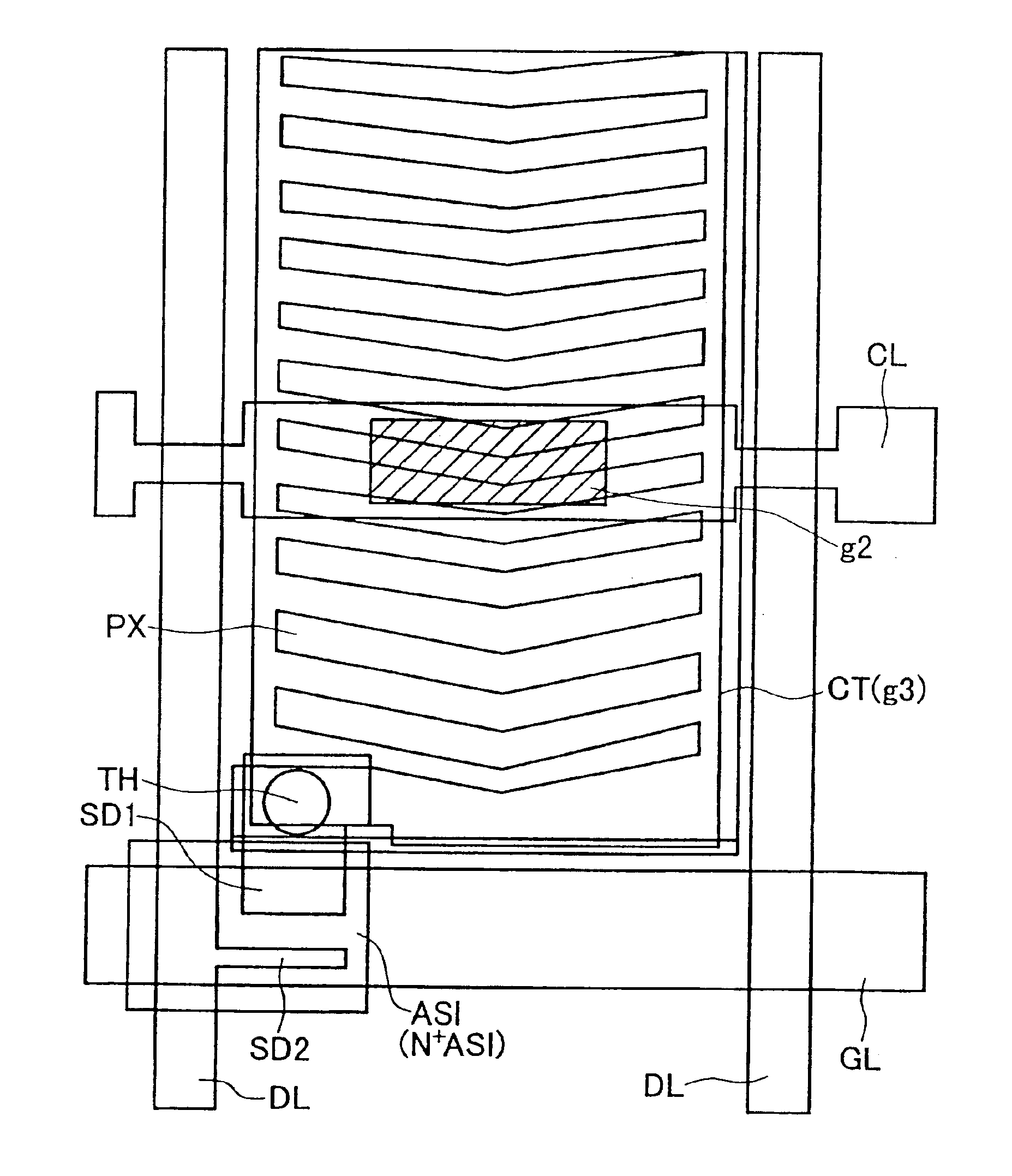
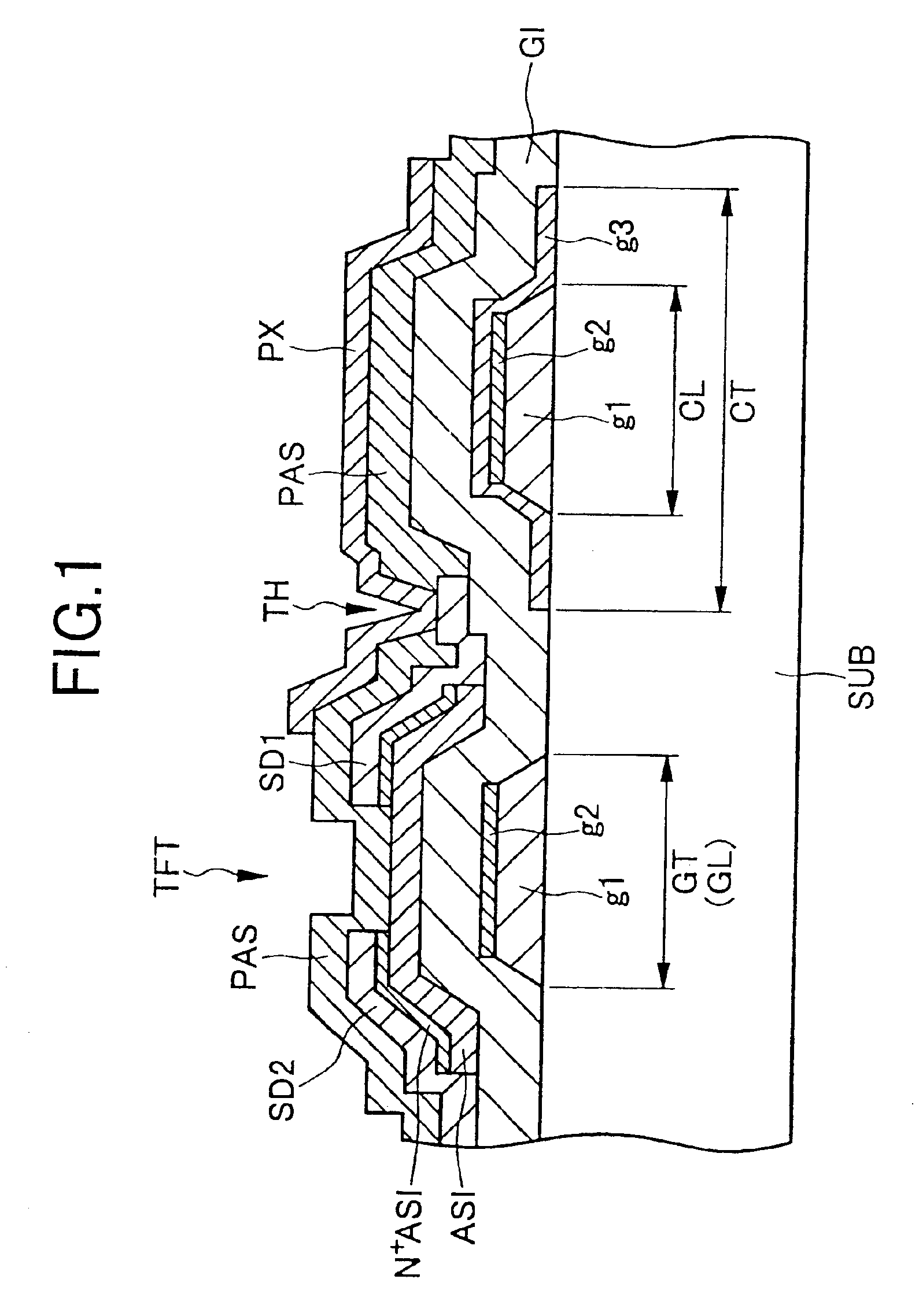
[0060]FIG. 1 is a diagrammatic cross-sectional view illustrating the construction of the essential portion of the liquid crystal display device according to the present invention, and diagrammatically shows a cross section of either one (a lower substrate) of insulative substrates disposed in opposition to each other with a liquid crystal interposed therebetween.

[0061]Referring to FIG. 1, a lower substrate SUB is suitably made of a glass substrate, and the inside surface of this lower substrate SUB has a gate line / electrode GT (GL) and a counter electrode / line CT (CL). The gate line / electrode GT (GL) is made of a stacked structure film of an aluminum alloy g1 and a molybdenum alloy g2, while the counter electrode / line CT (CL) is made of a stacked structure film which includes the aluminum alloy g1 and the molybdenum alloy g2 and is covered with a transparent conductive film g3 made of ITO. In FIG. 1, there are shown the gate electrode GT which constitutes a thin film transistor TFT,...

second embodiment

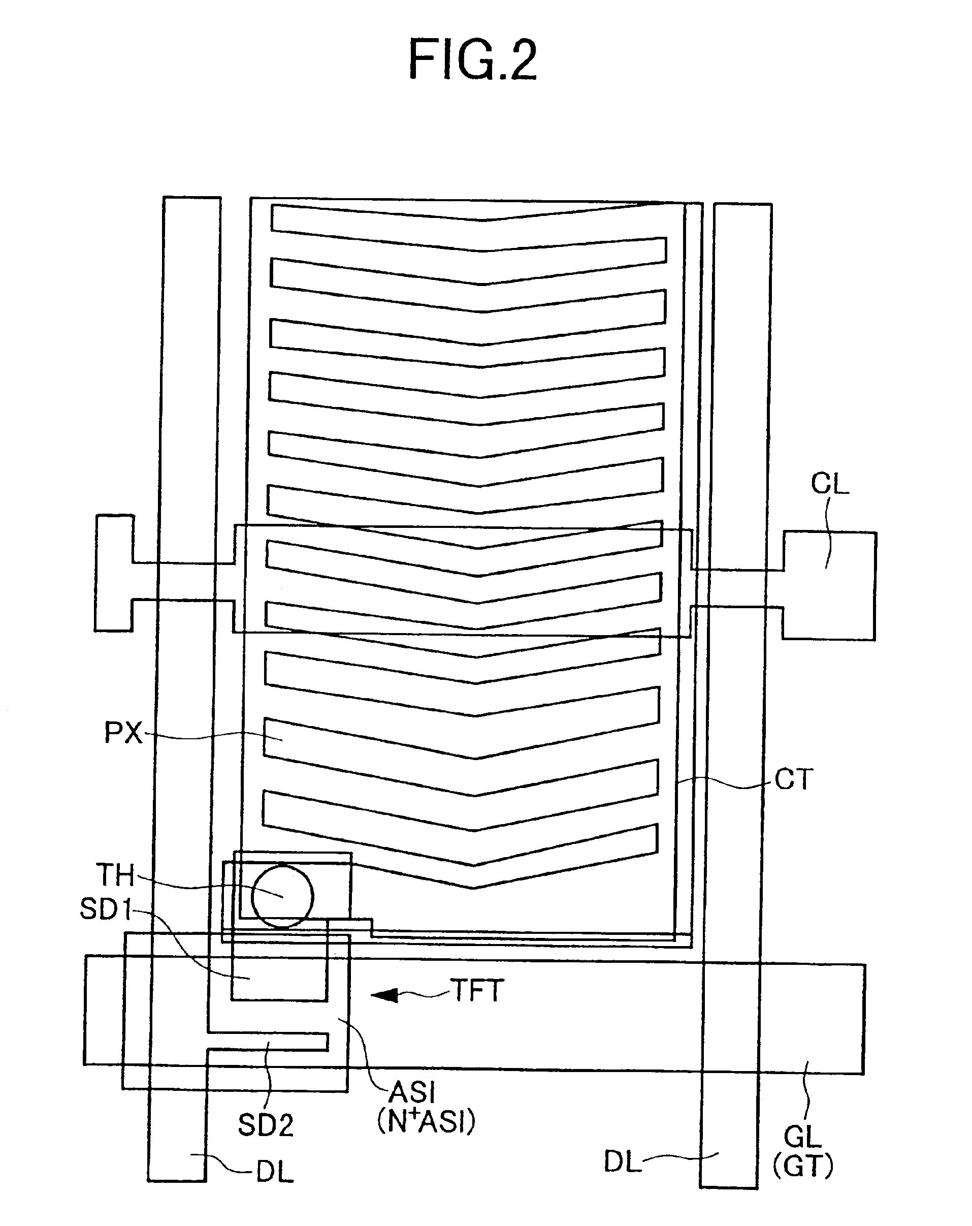
[0099]In the second embodiment, the counter electrode CT has a plane shape, but it may be processed into a comb-teeth like shape in the case of ordinary IPS mode.

[0100]The above-described ITO or the like is used as the amorphous transparent conductive film g3. A major part of the aluminum alloy (Al—Nd) film g1 which constitutes the gate line GL and the counter line CL is covered with the alumina film g4 so that the surface of neither of the aluminum film g1 and the counter electrode CT does not directly contact an etching solution. Accordingly, a crystalline transparent conductive film may also be used as the transparent conductive film g3.

[0101]After the formation of the counter electrode CT, the semiconductor layer ASI and the semiconductor layer N+ ASI which serves as a contact layer, the source electrode SD1, the drain line DL and the drain electrode SD2 are formed as shown in FIG. 11.

[0102]Furthermore, after the formation of the insulating film PAS, as shown in FIG. 12, a throu...

third embodiment

[0104]FIG. 13 is a diagrammatic cross-sectional view illustrating the construction of the essential portion of the liquid crystal display device according to the present invention, and diagrammatically shows a cross section of either one (a lower substrate) of insulative substrates disposed in opposition to each other with a liquid crystal interposed therebetween.

[0105]In the third embodiment, ITO or the like is formed on the inside surface of a TFT substrate SUB1 as an amorphous transparent conductive film g3. The counter line CL is made of a stacked structure film which has a chromium, molybdenum or titanium film g2 as a base (a lower layer) and an aluminum alloy (such as Al—Nd) film g1 as an upper layer.

[0106]Both the chromium, molybdenum or titanium film g2 which is the lower layer constituting the counter line CL and the amorphous transparent conductive film g3 which constitutes the counter electrode CT have good contact characteristics.

[0107]During etching treatment for patter...


PUM

PropertyMeasurementUnit
lengthaaaaaaaaaa
lengthaaaaaaaaaa
lengthaaaaaaaaaa

Abstract

An interconnecting structure and a pixel structure suited to large-sized screens are formed. A counter line / electrode is formed on a TFT substrate, and the counter line / electrode is made of a stacked structure film in which a layer made of aluminum or an alloy essentially containing aluminum is covered with a high-melting point metal film, and a transparent conductive film which covers the stacked structure film.

Description

CROSS-REFERENCES TO RELATED APPLICATIONS[0001]The present application is a Continuation Application of U.S. application Ser. No. 09 / 754,232, filed Jan. 3, 2001, which is related to and claims priority from Japanese Patent Application No. 2000-5856, filed on Jan. 7, 2000.BACKGROUND OF THE INVENTION[0002]The present invention relates to a liquid crystal display device and, more particularly, to a liquid crystal display device which is called In-Plane Switching mode.[0003]Liquid crystal display devices are widely used in various kinds of electronic equipment such as display devices such as display monitors for personal computers and television receivers. Various types of liquid crystal display devices are known. A liquid crystal display device of the type which is called In-Plane Switching (IPS) mode has a liquid crystal panel generally made of two substrates disposed in opposition to each other with a liquid crystal interposed therebetween. In each pixel area on the surface of either ...

Claims


Application Information

Patent Timeline
Patent Type & Authority Patents(United States)
IPC IPC(8): G02F1/13G02F1/1362G02F1/1343G02F1/133G09F9/30G02F1/136G02F1/1368
CPCG02F1/134363G02F1/136286G02F2203/01G02F2001/136295G02F2201/123G02F2001/13629G02F1/13629G02F1/136295G02F1/133
Inventor KANEKO, TOSHIKIFUJII, KAZUMIONO, KIKUO
Owner PANASONIC LIQUID CRYSTAL DISPLAY CO LTD
Why Eureka
Try Eureka