Optical waveguide sensor, device, system and method for glucose measurement

a technology of optical waveguide and glucose sensor, which is applied in the field of optical waveguide type glucose sensor, can solve the problems of limiting the sensitivity of detecting the change in the quantity of evanescent wave generated, and the film structure of the optical waveguide layer is not suitable for analysis of the extremely small amount of biomolecules contained in blood

Inactive Publication Date: 2005-06-07
KK TOSHIBA
View PDF16 Cites 34 Cited by
  • Summary
  • Abstract
  • Description
  • Claims
  • Application Information

AI Technical Summary

Problems solved by technology

However, in the conventional glucose sensor there have been problems, such as, since the optical waveguide layer is made up with a single layer, there is a limit to the sensitivity in detecting the change in the quantity of the evanescent wave generated in the optical waveguide layer, and also the film structure on the optical waveguide layer is not suitable for analysis of the extremely small amounts of biomolecules contained in blood and the like which are extracted from the analyte.

Method used


Image

  • Optical waveguide sensor, device, system and method for glucose measurement
  • Optical waveguide sensor, device, system and method for glucose measurement
  • Optical waveguide sensor, device, system and method for glucose measurement

Examples


first embodiment

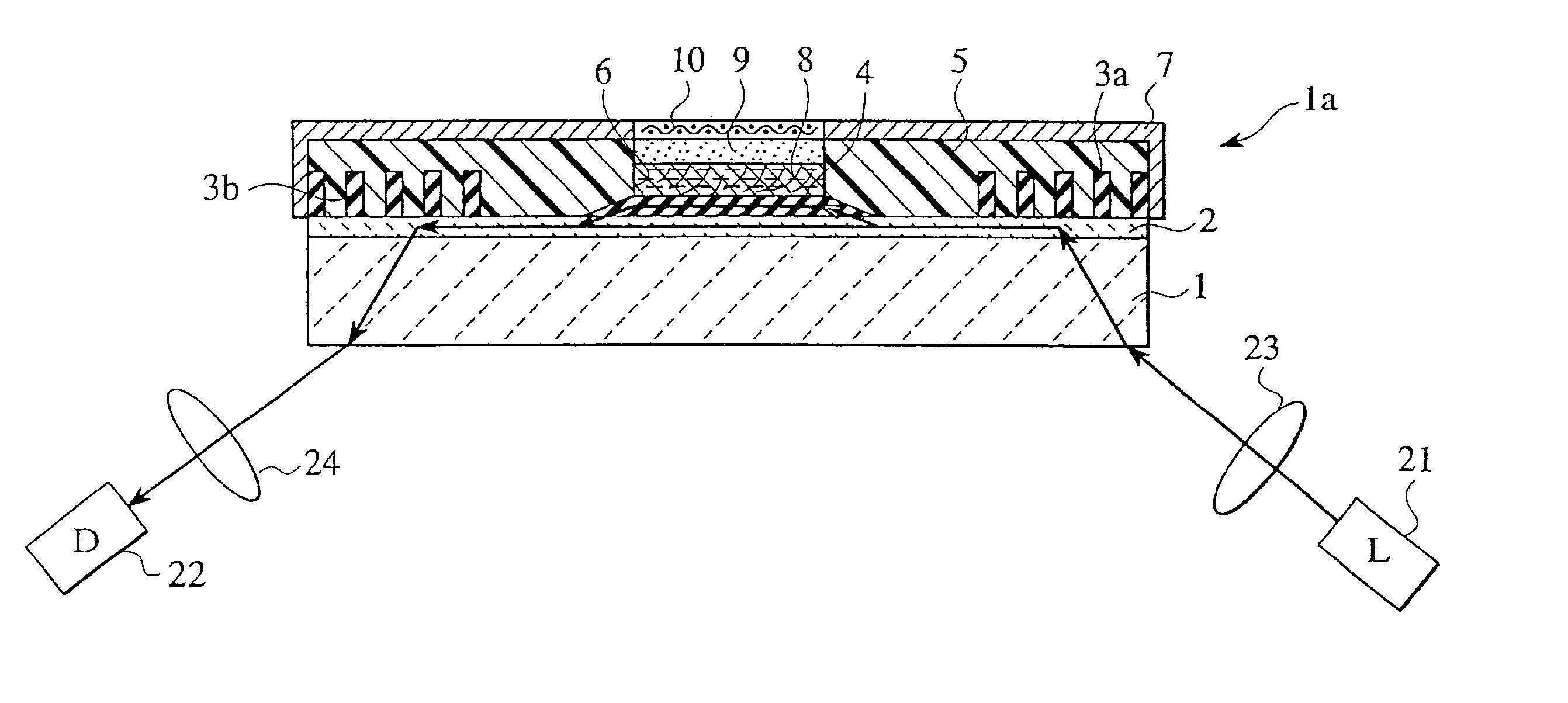
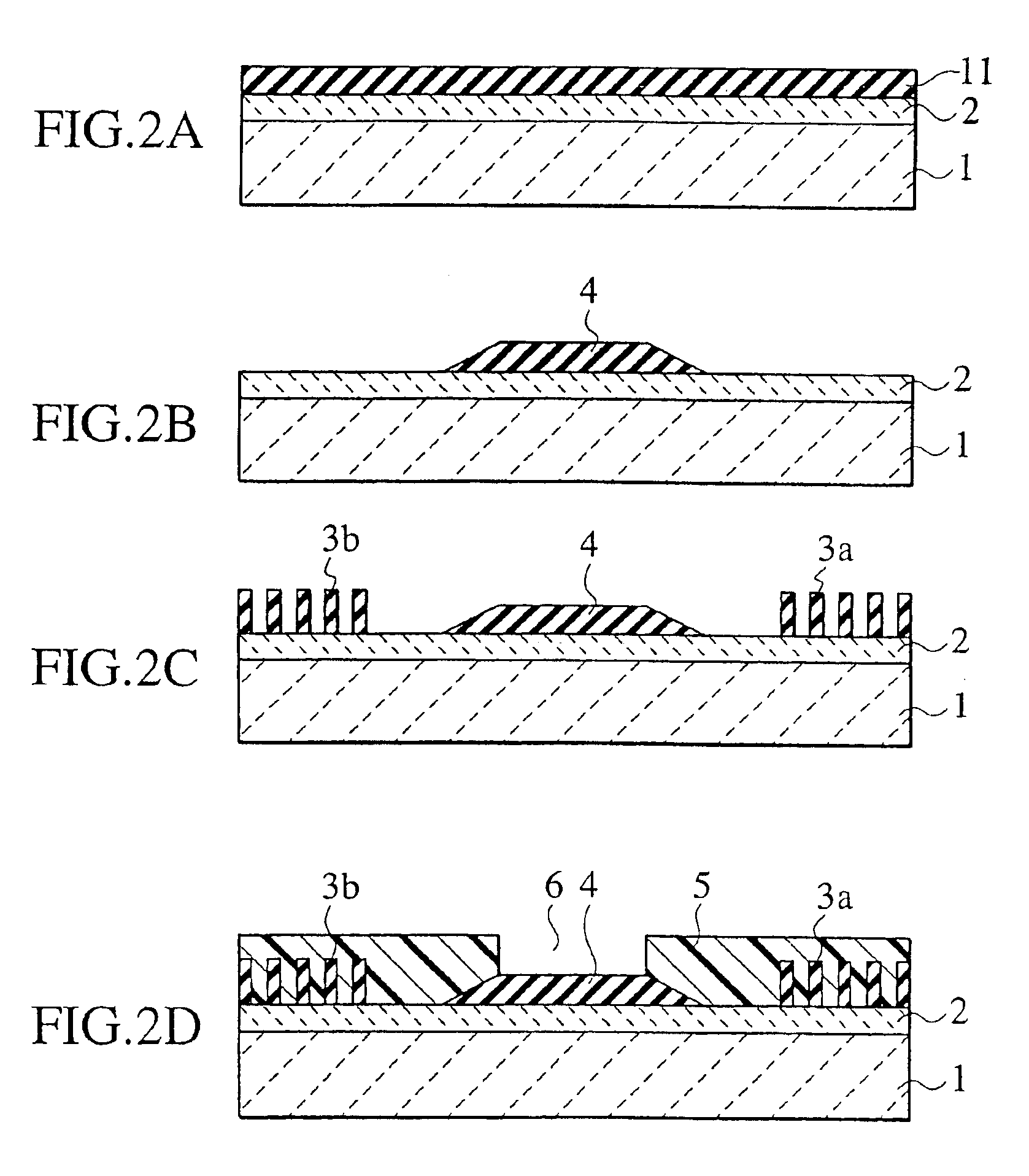
[0035]In an optical waveguide type glucose sensor 1a according to the first embodiment of the present invention, as illustrated in FIG. 1, a substrate 1 which is made of glass, for example, and a first optical waveguide layer 2 having a refractive index higher than that of the substrate 1 and being placed on the surface of the substrate 1, are formed. In addition, a grating 3a located at an entrance portion (hereinafter the entrance grating) and another grating 3b located at an exit portion (hereinafter the exit grating) have refractive indexes higher than that of the first optical waveguide layer 2, and both gratings are respectively formed on the surface in the vicinities of both ends of the first optical waveguide layer 2. Moreover, the second optical waveguide layer 4 in which a circumference is tapered in shape and has a higher refractive index than the first optical waveguide layer 2 and is formed on a part of the first optical waveguide layer 2, is located between the entranc...

second embodiment

[0059]The optical waveguide type glucose sensor 1b illustrated in FIG. 4 has a structure in which an immobilized coloring reagent layer 13 is formed on the second optical waveguide layer 4 and an immobilized enzyme layer 14 is formed on the immobilized coloring reagent layer 13. In short, the optical waveguide type glucose sensor 1b shown in FIG. 4 has a structure in which the functioning layer 8 in the previously mentioned first embodiment is separated into two layers, the immobilized coloring reagent layer 13 and the immobilized enzyme layer 14.

[0060]The immobilized coloring reagent layer 13 is formed by fixing the coloring reagent to the surface of the second optical waveguide layer 4 by the application of silane coupling agent or cross-linking polymer, wherein examples of the coloring reagent are dipotassium N. N-bis(2-hydroxy-3-sulfopropyl)tolidine salt or 3,3′,5,5′-tetramethylbenzidine, an example of the silane coupling agent is aminoalkyltrimethoxysilane, and an example of th...

third embodiment

[0064]An optical waveguide type glucose sensor 1c illustrated in FIG. 5 has a second optical waveguide layer 15 on the first optical waveguide layer 2 between the entrance grating 3a and the exit grating 3b. The second optical waveguide layer 15 is formed by an electro-conductive material having a refractive index higher than that of the first optical waveguide layer 2 such as stannum oxide (SnO2) and ITO, and a desired electric field (for example, a pulsed electric field) is applied to the second optical waveguide layer 15.

[0065]As a modification of wiring shown in FIG. 3, the cathode of an electric source 102 is wired to the second optical waveguide layer 15, and the anode of the electric source 102 is wired to an electrode plate 101 in the optical waveguide type glucose sensor 1c illustrated in FIG. 5. Then, the analyte 100, for example, a part of a human skin, is placed to contact with the portion of the porous film 9 provided on the functioning layer 8 containing the enzyme and...


PUM

PropertyMeasurementUnit
wave lengthaaaaaaaaaa
refractive indexaaaaaaaaaa
electro-conductiveaaaaaaaaaa

Abstract

An optical waveguide sensor for glucose measurement comprises a substrate, a first optical waveguide layer formed on a surface of the substrate, an entrance grating and an exit grating which are formed contacting with the first optical waveguide layer and being spaced from each other, a second optical waveguide layer located between the entrance grating and the exit grating while being in contact with the first optical waveguide layer, the second optical waveguide layer having a higher refractive index that that of the first optical waveguide layer, and a functioning layer containing an enzyme and a coloring reagent which is formed on the second optical waveguide layer.

Description

CROSS REFERENCE TO RELATED APPLICATIONS[0001]This application is based upon and claims the benefit of priority from the prior Japanese Patent Applications No. P2001-358333, filed on Nov. 22, 2001, No. P2002-7807, filed on Jan. 16, 2002, No. P2002-7808, filed on Jan. 16, 2002 and No. P2002-140055, filed on May 15, 2002; the entire contents of which are incorporated herein by reference.BACKGROUND OF THE INVENTION[0002]1. Field of the Invention[0003]The present invention relates to a glucose sensor, and especially relates to an optical waveguide type glucose sensor, a device for optical waveguide type glucose measurement, a system for optical waveguide type glucose measurement and a methodology for optical waveguide type glucose measurement for measuring glucose concentration in a solution such as blood.[0004]2. Description of the Related Art[0005]In the Japanese Patent Laid-Open Publication No. Hei 9 (1997)-61346, for example, a planar optical waveguide type glucose sensor has been di...

Claims


Application Information

Patent Timeline
Patent Type & Authority Patents(United States)
IPC IPC(8): A61B5/00C12Q1/00G01N21/77G01N21/78G01N33/543
CPCA61B5/14525A61B5/14532A61B5/1455C12Q1/006G01N21/78G01N33/54373G01N21/7703A61B2562/12G01N2021/7783G01N2021/7709G01N2021/773G01N2021/7779
Inventor UCHIYAMA, KENICHITONO, ICHIROETO, HIDEONAGATOMO, MIKI
Owner KK TOSHIBA
Why Eureka
Try Eureka