Floating-body DRAM using write word line for increased retention time

a floating-body dram and memory cell technology, applied in the field of memory circuits, can solve the problems of low memory cell density, significant limitation of the performance of the microprocessor system, and die spa

Inactive Publication Date: 2005-06-07
INTEL CORP
View PDF2 Cites 141 Cited by
  • Summary
  • Abstract
  • Description
  • Claims
  • Application Information

AI Technical Summary

Problems solved by technology

This six-transistor configuration consumes considerable die space and thus leads to low memory cell density.
This, in turn, places a significant limitation on microprocessor system performance, and for at least these reasons using SRAM cells to fabricate on-die caches is considered to be less than optimal.
While they are favored, conventiona...

Method used


Image

  • Floating-body DRAM using write word line for increased retention time
  • Floating-body DRAM using write word line for increased retention time
  • Floating-body DRAM using write word line for increased retention time

Examples


Embodiment Construction

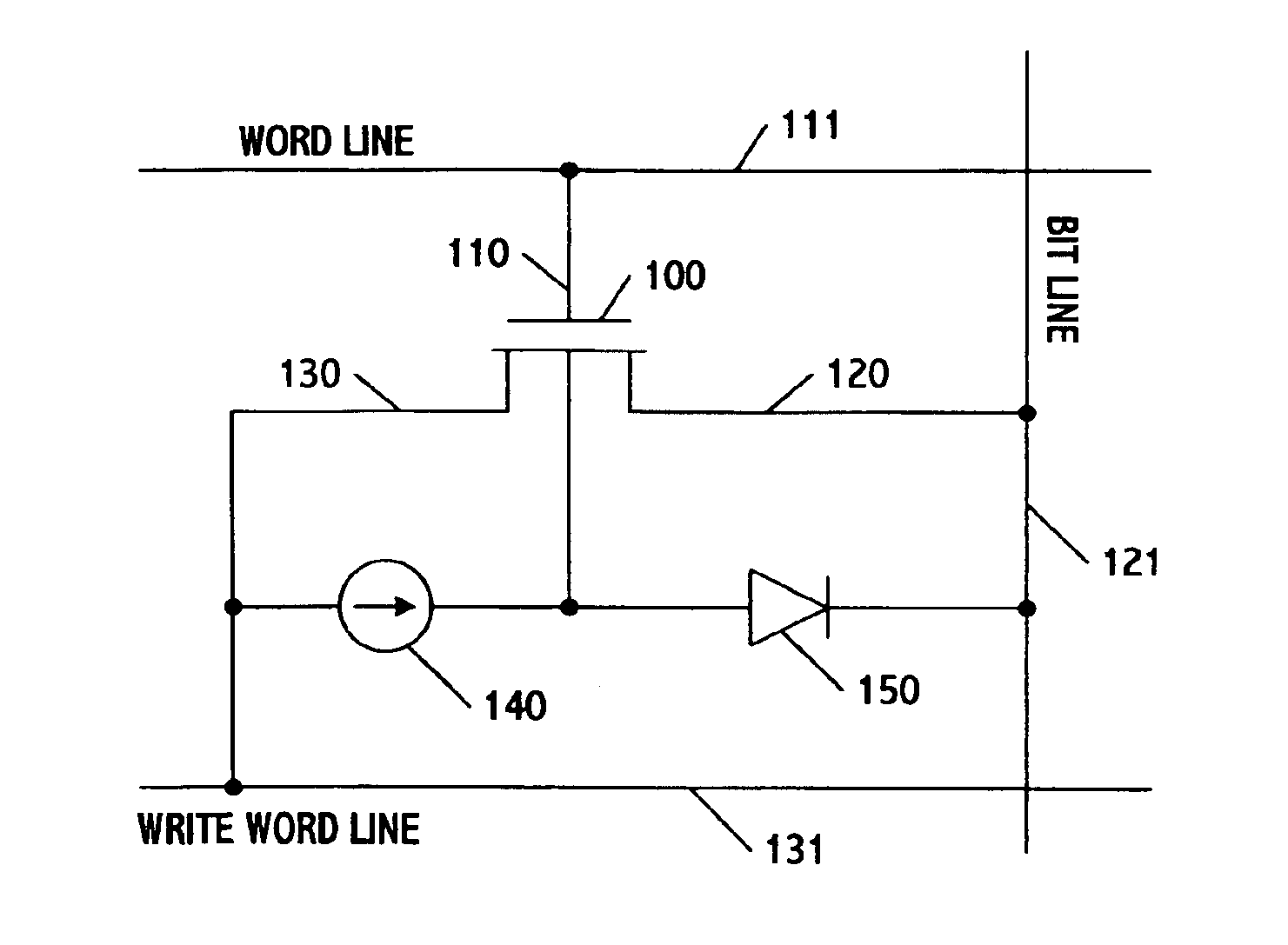
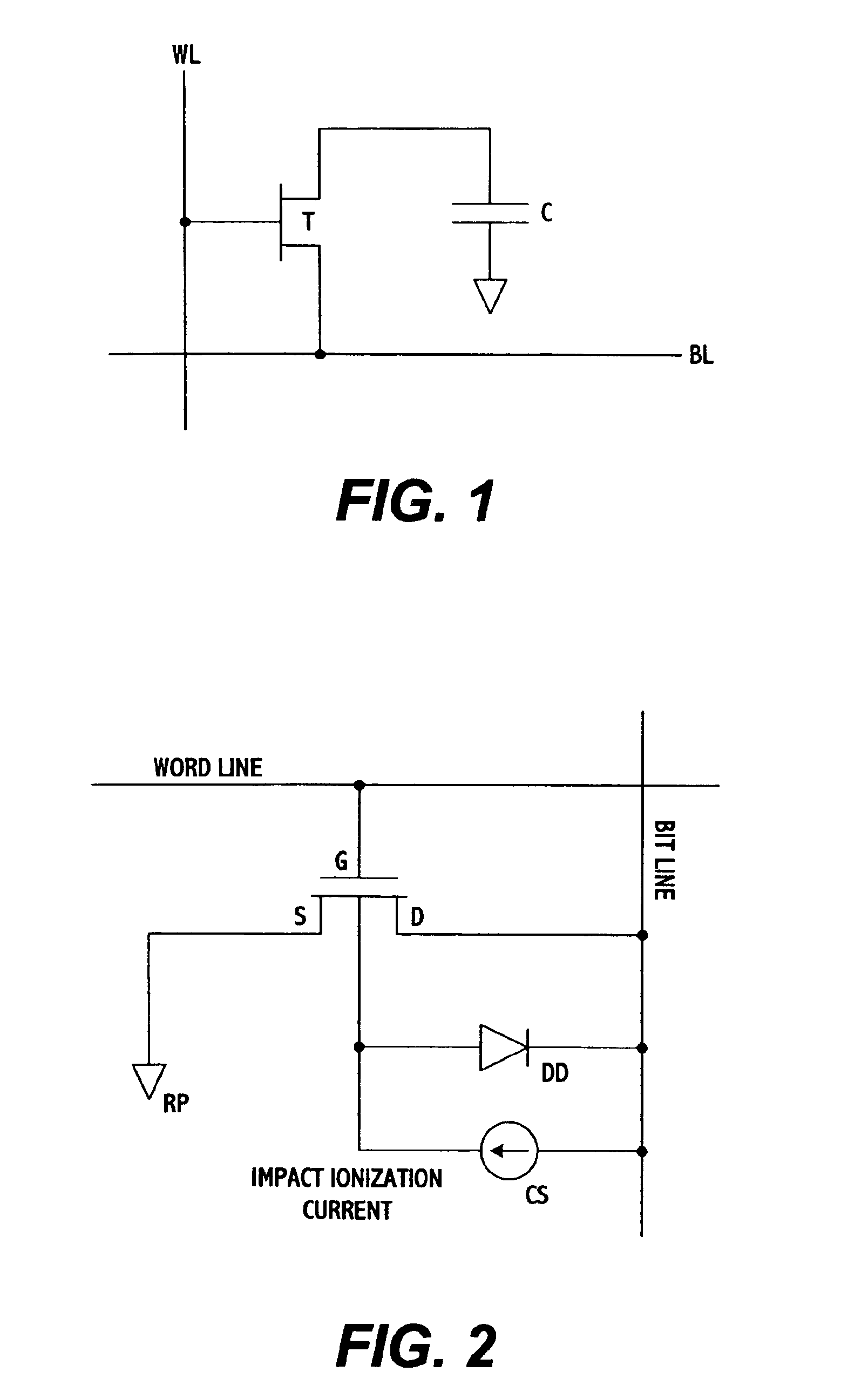
[0024]FIG. 2 is a diagram showing a first type of DRAM gain cell having a floating-body structure. The cell is formed from a single transistor having a source S connected to a reference potential RP (e.g., ground), a drain D connected to a bit line, and a gate G connected to a word line. A diode DD is provided to show a direction in which the drain junction is forward biased during a write ′0″ operation, and a current source CS is provided to show the direction in which impact ionization current flows when the transistor operates in a saturated operating region (i.e., when the drain voltage is greater than the gate voltage minus the threshold voltage, Vg−VT) during a write ′1″ operation. As will become more apparent below, DD and CS are inherent to the transistor structure and are shown in FIG. 2 for explanatory purposes only.

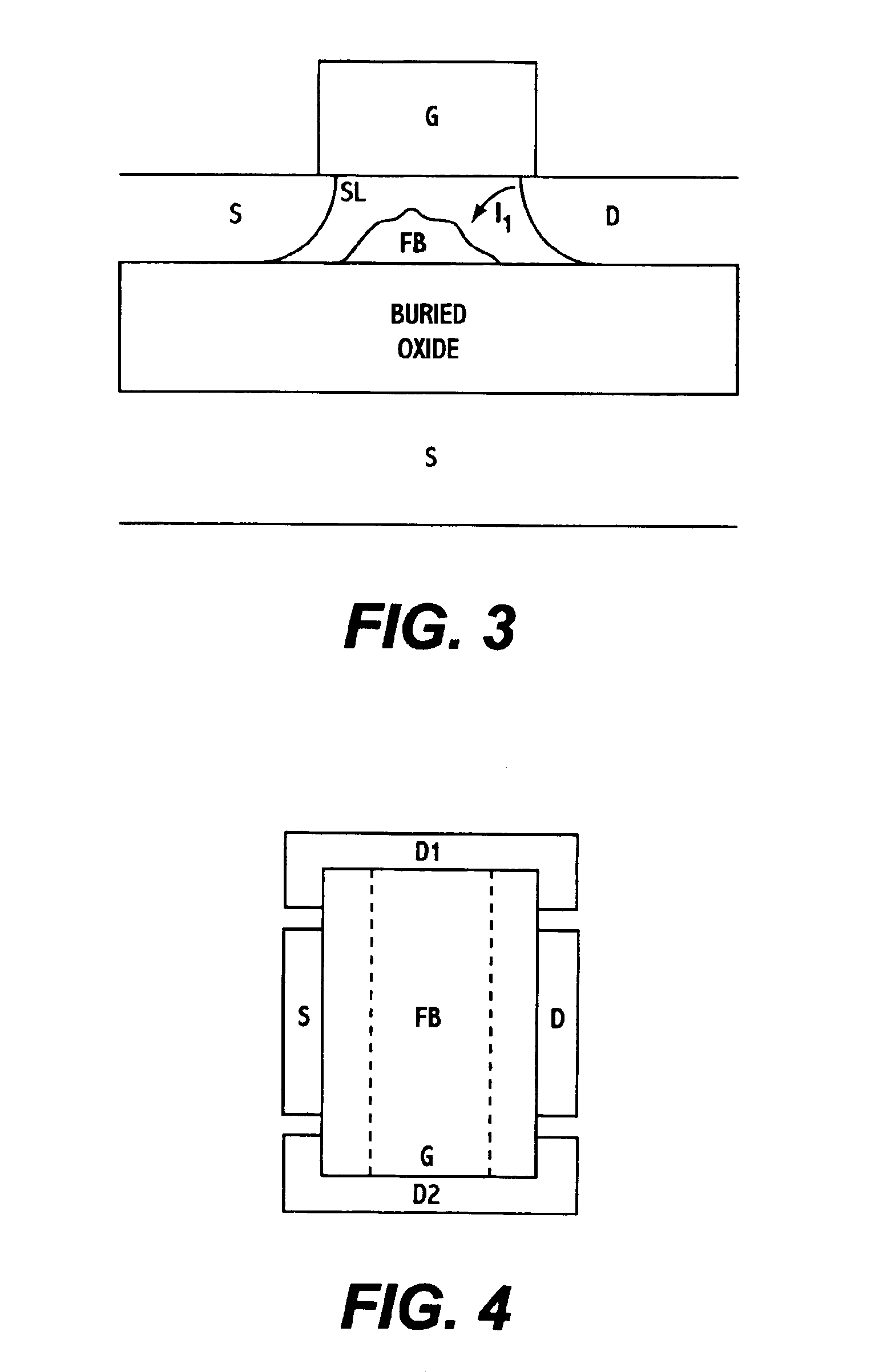
[0025]The transistor has an silicon-on-insulator (SOI) structure which, as shown in FIG. 3, includes an insulating layer (e.g., SiO2) formed on a silicon subst...


PUM


Abstract

A DRAM memory cell uses a single transistor to perform the data storage and switching functions of a conventional cell. The transistor has a floating channel body which stores a potential that corresponds to one of two digital data values. The transistor further includes a gate connected to a first word line, a drain connected to a second word line, and a source connected to a bit line. By setting the word and bit lines to specific voltage states, the channel body stores a digital one potential as a result of impact ionization and a digital zero value as a result of forward bias of body-to-source junction.

Description

BACKGROUND OF THE INVENTION[0001]1. Field of the Invention[0002]This invention relates to memory circuits, and more particularly to a memory cells formed from floating-body transistors and their applications.[0003]2. Description of the Related Art[0004]Integrating memory circuits (e.g., caches) on microprocessor dies is a power efficient way of achieving higher performance. In fabricating these dies, a direct correlation exists between memory cell density and performance; that is, performance generally increases with the number of cells in the memory. The degree of integration that can be achieved is not limitless and most often is constrained by memory type, the limited die space available for accommodating the memory circuits, and manufacturing costs as well as other practical considerations.[0005]One memory type that has been proposed for integration onto a microprocessor die is SRAM memory. When implemented in large caches, each SRAM memory cell uses six transistors to read and ...

Claims


Application Information

Patent Timeline
IPC IPC(8): G11C11/404G11C11/408G11C11/403H01L27/108H01L29/78
CPCG11C11/404H01L29/7841H01L27/108G11C11/4085H10B12/00
Inventor TANG, STEPHENKESHAVARZI, ALISOMASEKHAR, DINESHPAILLET, FABRICEKHELLAH, MUHAMMADYE, YIBINDE, VIVEK
Owner INTEL CORP
Why Eureka
Try Eureka