Vertical cavity surface emitting laser having a gain guide aperture interior to an oxide confinement layer

a laser and gain guide technology, applied in semiconductor lasers, laser details, optical resonator shape and construction, etc., can solve the problems of low threshold, inability to produce significant optical guiding, and inability to achieve significant optical guiding by ion implantation. achieve the effect of low threshold and high efficiency

Inactive Publication Date: 2005-06-07
II VI DELAWARE INC
View PDF25 Cites 10 Cited by
  • Summary
  • Abstract
  • Description
  • Claims
  • Application Information

AI Technical Summary

Benefits of technology

[0019]Accordingly, the principles of the present invention are directed to a new VCSEL that possess benefits of both ion implanted and oxide VCSELs. According to the principles of the present invention, an oxide structure and an interior gain guide ion implant structure are combined to form a VCSEL. The combination of the oxide layer and an interior ion implant gain guide can achieve desirable low order optical modes with low threshold and high efficiency. To support fewer optical modes the oxide layer is formed more than two mirror periods from the active region. Beneficially, the oxide layer has an optical thickness less than ¼ wavelength.

Problems solved by technology

While generally successful, VCSELs have problems.
However, prior art insulating regions 40 are less than optimal in producing single mode light.
That proton implantation creates structural defects that produce a relatively high resistance annular structure having a conductive core.
While the high resistance annular structure effectively steers current through its conductive core and into the active region, ion implantation does not produce significant optical guiding.
The result is that ion implantation is effective at steering current into the active region, but ineffective at limiting the optical modes of the laser.

Method used


Image

  • Vertical cavity surface emitting laser having a gain guide aperture interior to an oxide confinement layer
  • Vertical cavity surface emitting laser having a gain guide aperture interior to an oxide confinement layer
  • Vertical cavity surface emitting laser having a gain guide aperture interior to an oxide confinement layer

Examples


Embodiment Construction

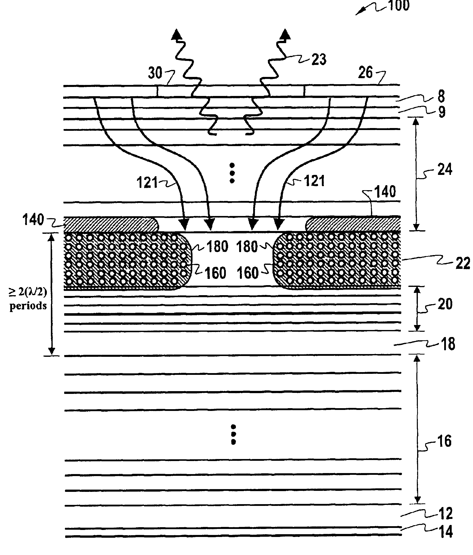
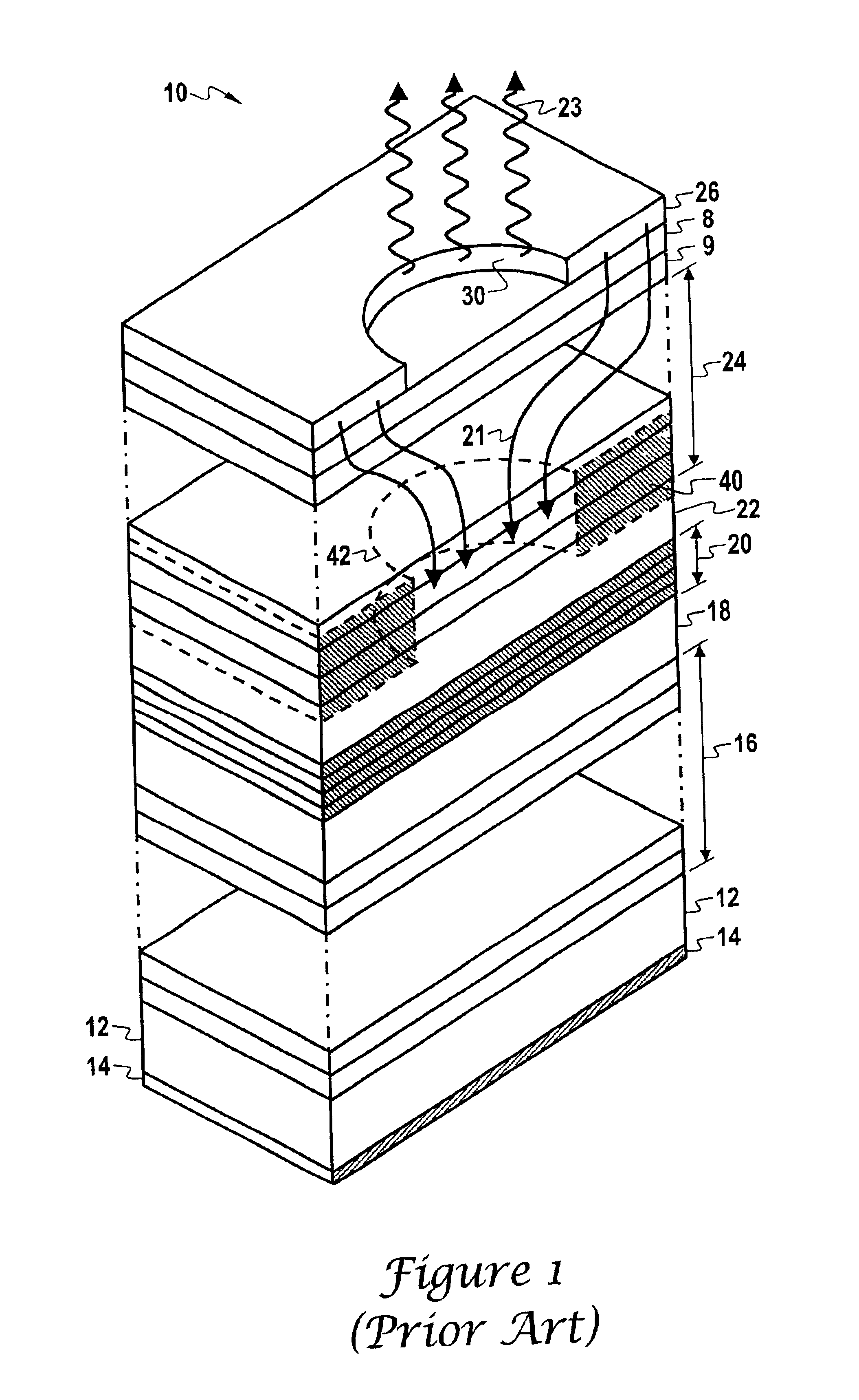
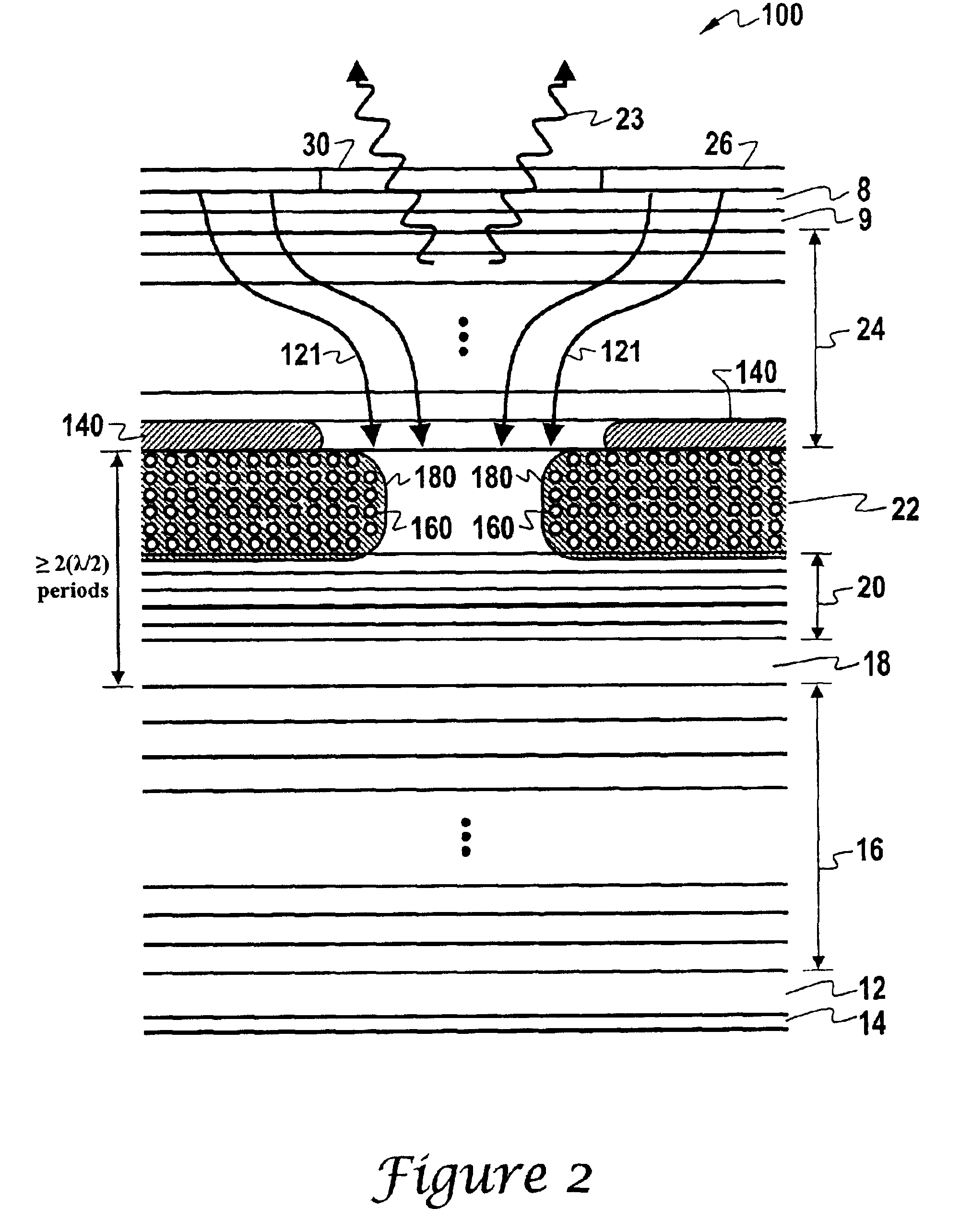
[0026]The principles of the present invention provide for a VCSEL that uses a current confinement structure comprised of an oxide structure and an interior gain guide ion implant structure. An example of such a VCSEL is the VCSEL 100 illustrated in FIG. 2. FIG. 2 should be understood as a “cut-away” schematic depiction of layers of a VCSEL that is generally configured as shown in FIG. 1. Thus, the same element numbers will be used for similar elements in FIG. 2 that were used in FIG 1.

[0027]Although for clarity our description of the illustrated embodiment assumes a VCSEL with mirrors and active region based on the AlGaAs material system, the invention broadly applies to VCSELs using any commensurate material system, such as AlGaAs mirrors and AlGaInP / GaAs active region for 670 nm, or AlGaInAs / InP mirrors and AlGaInAs active region for 1550 nm.

[0028]As shown in FIG. 2, the VCSEL 100 includes an n-doped gallium arsenide (GaAS) substrate 12 having an n-type electrical contact 14. An n...


PUM


Abstract

A VCSEL with current confinement achieved by an oxide insulating region and by an ion implant region. An annular shaped oxide layer is formed, and a gain guide ion implant is formed. The ion implant gain guide includes a central region having high conductivity. The VCSEL further includes first and second mirrors that are separated by an optical path of at least one wavelength. Furthermore, the oxide insulating region beneficially has a optical path of less than ¼ wavelength. The ion implanted spatial region is beneficially concentrically aligned with the oxide insulating region.

Description

UNITED STATES GOVERNMENT RIGHTS[0001]The United States Government has acquired certain rights in this invention through Government Contract No. 70NANB5H1114 awarded by NIST ATP.CROSS-REFERENCE TO RELATED APPLICATIONS[0002]Not applicable.BACKGROUND OF THE INVENTION[0003]1. Field of the Invention[0004]The present invention relates generally to the field of vertical cavity surface emitting lasers. More specifically, it relates to current confinement structures used in vertical cavity surface emitting lasers.[0005]2. Discussion of the Related Art[0006]Vertical cavity surface emitting lasers (VCSELs) represent a relatively new class of semiconductor lasers. While there are many variations of VCSELs, one common characteristic is that they emit light perpendicular to a wafer's surface. Advantageously, VCSELs can be formed from a wide range of material systems to produce specific characteristics.[0007]VCSELs include semiconductor active regions, which can be fabricated from a number of mate...

Claims


Application Information

Patent Timeline
Patent Type & Authority Patents(United States)
IPC IPC(8): H01S5/00H01S5/183H01S5/20
CPCH01S5/18333H01S5/18308H01S5/18311H01S5/2063H01S5/18358
Inventor COX, JAMES A.STRZELECKA, EVA
Owner II VI DELAWARE INC
Why Eureka
Try Eureka