Photomask for reducing power supply voltage fluctuations in an integrated circuit and integrated circuit manufactured with the same

a technology of power supply voltage fluctuations and photomasks, which is applied in the field of photolithography, can solve the problems of false switching of logic gates, additional signal delay, ringing in the output waveform or delay in response speed, etc., and achieve the effect of substantially reducing or eliminating the disadvantages and problems of reducing power supply voltage fluctuations in the integrated circui

Inactive Publication Date: 2005-06-07
CELERICS TECH
View PDF7 Cites 219 Cited by
  • Summary
  • Abstract
  • Description
  • Claims
  • Application Information

AI Technical Summary

Benefits of technology

[0006]In accordance with the present invention, the disadvantages and problems associated with reducing power supply voltage fluctuations in an integrated circuit have been substantially reduced or eliminated. In a particular embodiment, a photomask is formed by using a mask pattern file created by automatically moving a feature located in an identified region of a mask layout file from a first position to a second position based on a design rule to create a space for one or more decoupling capacitors.
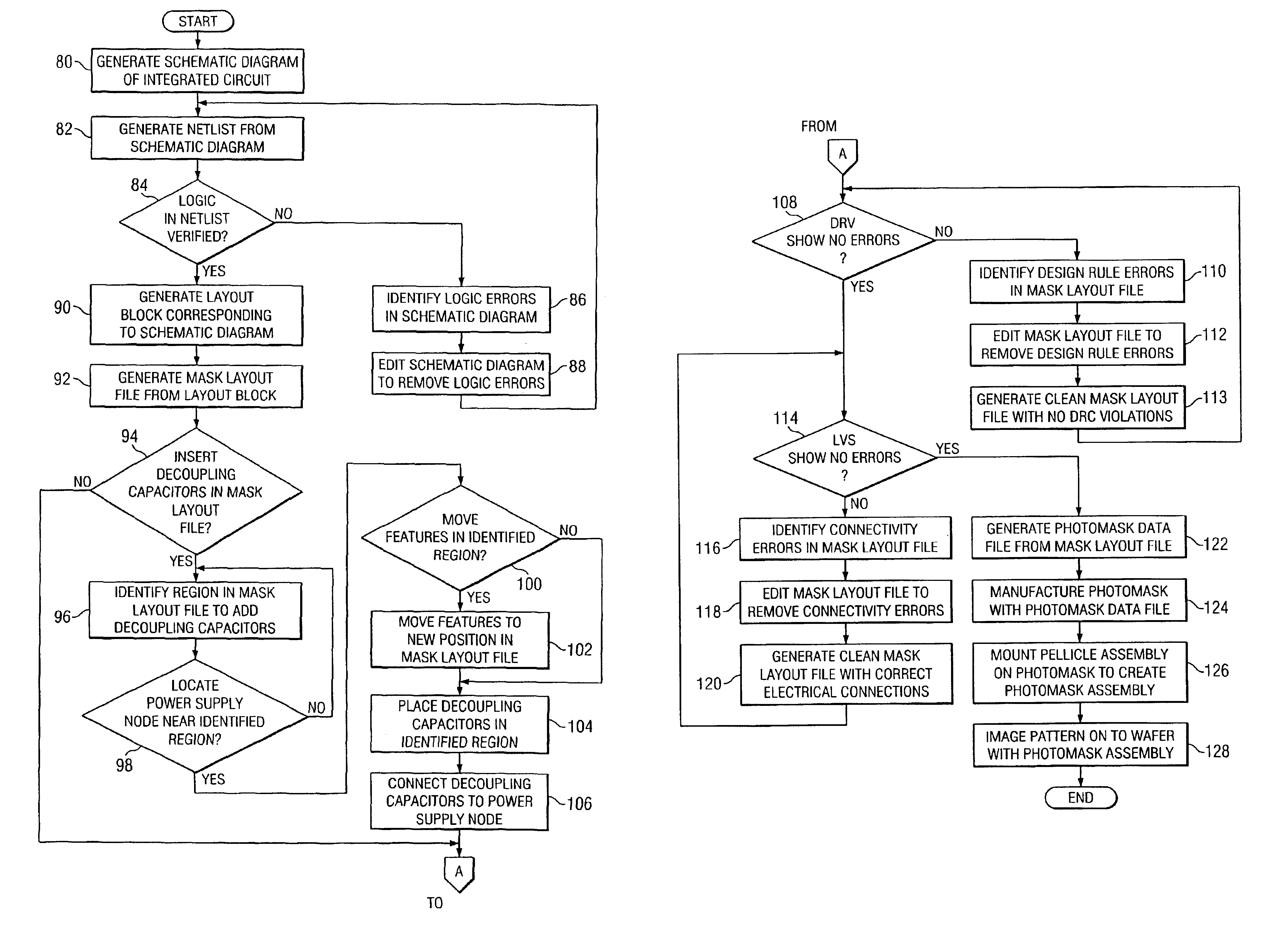
[0009]Important technical advantages of certain embodiments of the present invention include a placement tool that automatically connects decoupling capacitors added to a mask layout file to a power supply node. The placement tool analyzes the mask layout file to identify valid or empty regions to place decoupling capacitors. Before placing the capacitors, the placement tool determines if a connection may be established from the decoupling capacitors to the power supply. If the connection may be established, the placement tool automatically moves any features to create a routing path for the connection and simultaneously eliminates or prevents design rule violations and / or connectivity errors from being created.
[0010]Another important technical advantage of certain embodiments of the present invention includes a placement tool that reduces the amount of time required to design and manufacture a semiconductor device. During placement of the capacitors in a mask layout file, the placement tool invokes a design rule fix (DRF) tool and a layout versus schematic (LVS) tool to respectively correct design rule violations and connectivity errors. Since the placement and correction processes occur together, the mask layout file may be free of design rule violations in a shorter amount of time, which reduces the cycle time for manufacturing a photomask used to fabricate the semiconductor device.

Problems solved by technology

However, spike currents generated during switching can cause power (VCC) and ground (GND) voltage levels to fluctuate, which may cause ringing in the output waveform or a delay in response speed.
This power supply noise not only will introduce additional signal delay, but also may cause false switching of logic gates.
The selected locations of the decoupling capacitors in the mask layout database, however, may not be optimal and thus, the use of space in the mask layout database may be inefficient.
The layout designer may inadvertently create design rule violations or connectivity errors.
The process of iteratively correcting the design rule violations may take several hours or even days to complete and can increase the time needed to design the integrated circuit.
The additional time required to complete layout may also delay the production of a photomask set used to fabricate the integrated circuit.

Method used


Image

  • Photomask for reducing power supply voltage fluctuations in an integrated circuit and integrated circuit manufactured with the same
  • Photomask for reducing power supply voltage fluctuations in an integrated circuit and integrated circuit manufactured with the same
  • Photomask for reducing power supply voltage fluctuations in an integrated circuit and integrated circuit manufactured with the same

Examples


Embodiment Construction

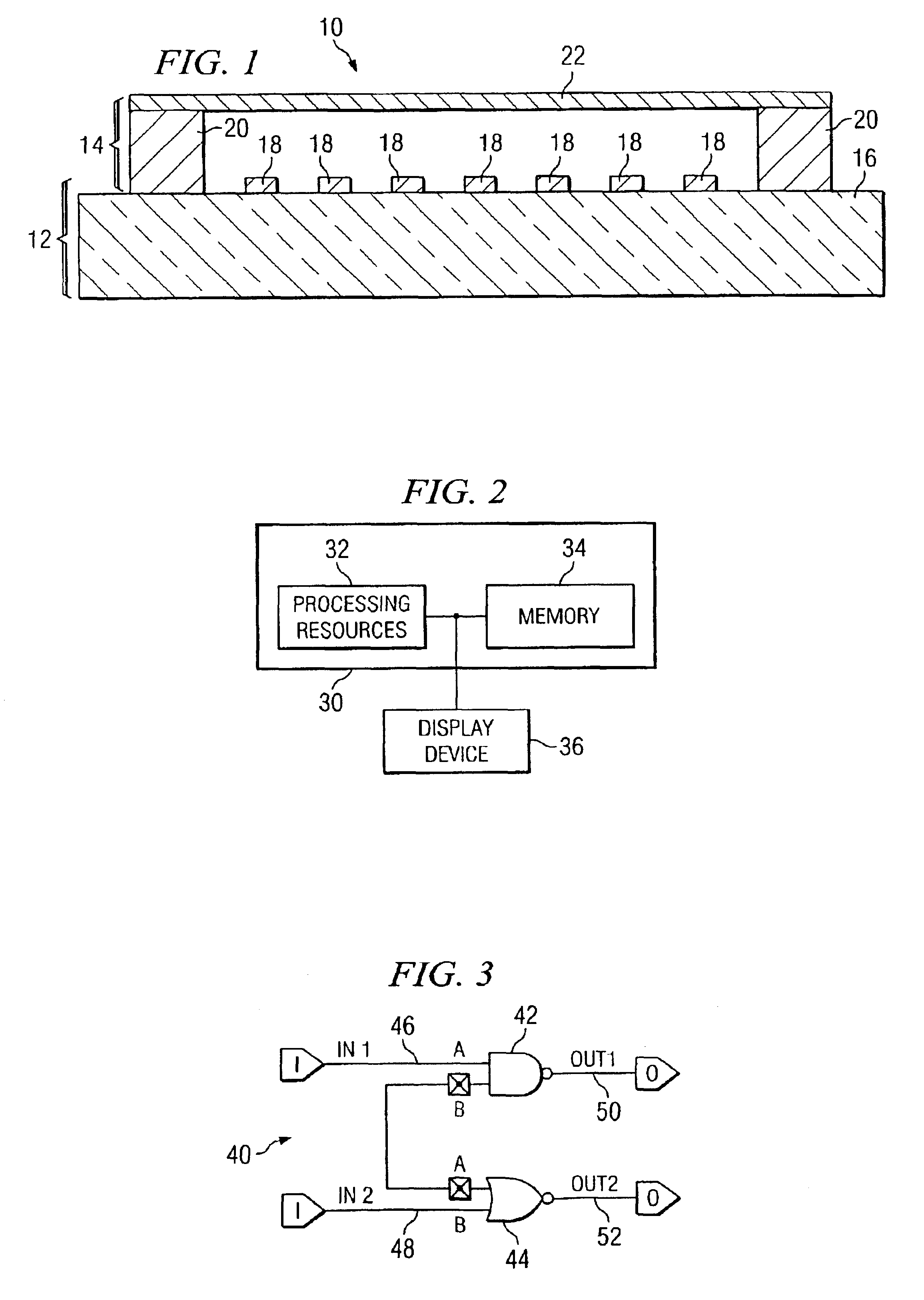
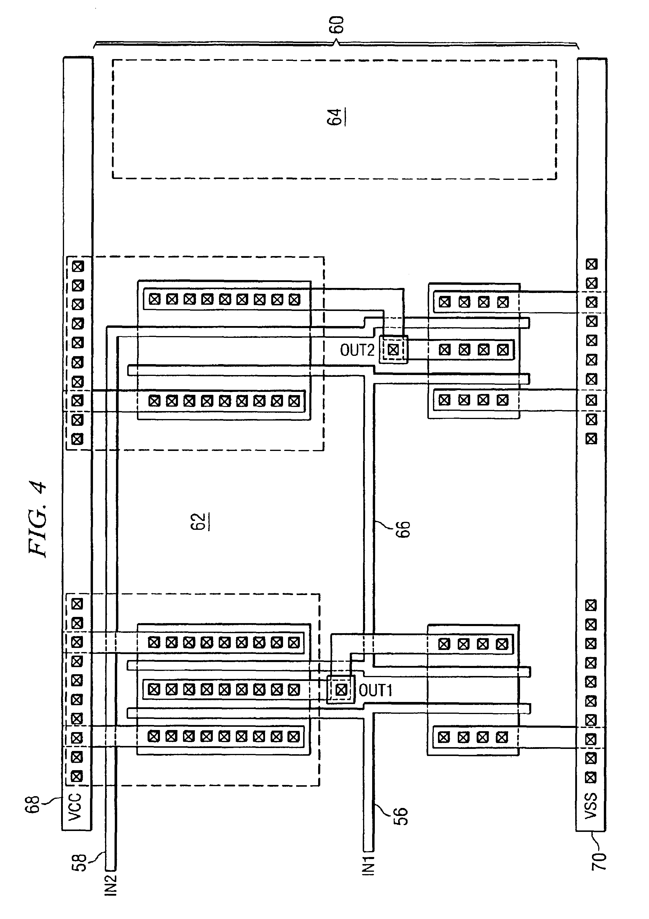
[0019]Preferred embodiments of the present invention and their advantages are best understood by reference to FIGS. 1 through 6, where like numbers are used to indicate like and corresponding parts.

[0020]As the number of transistors on an integrated circuit (IC) continues to increase, the design process for the IC becomes more complex. For example, an increasing number of transistors may require additional layers to form the IC on a semiconductor wafer. Each layer associated with the IC may include one or more design rules for the individual layer in a desired manufacturing process. The number of design rules for the desired manufacturing process, therefore, increases with the number of layers formed on the semiconductor wafer.

[0021]A design rule typically defines the minimum or maximum allowable dimension for a feature fabricated on a specific layer. For example, an IC may include, among other layers, a diffusion layer that forms a decoupling capacitor and / or the source and drain r...


PUM

PropertyMeasurementUnit
transparentaaaaaaaaaa
wavelengthaaaaaaaaaa

Abstract

A photomask for reducing power supply voltage fluctuations in an integrated circuit and integrated circuit manufactured by the same are disclosed. The photomask includes a substrate and a patterned layer formed on at least a portion of the substrate. The patterned layer may be formed using a mask pattern file created by analyzing a pattern in a mask layout file to identify a region in the pattern to add one or more decoupling capacitors. Once the region is identified, a feature located in the identified region is moved based on a design rule from a first position to a second position in the mask layout file to create a space in the identified region. The decoupling capacitors are placed in the space in the identified region.

Description

RELATED APPLICATIONS[0001]This application is a continuation-in-part of U.S. patent application Ser. No. 10 / 084,216, filed Feb. 28, 2002 and entitled “AUTOMATIC PLACEMENT AND CONNECTION OF DECOUPLING CAPACITORS THROUGHOUT MASK LAYOUT DATABASE (IC LAYOUT), ACCORDING TO PROCESS DESIGN RULES AND SCHEMATIC CONNECTIVITY, METHOD AND COMPUTER SOFTWARE” now abandoned.TECHNICAL FIELD OF THE INVENTION[0002]This invention relates in general to the field of photolithography, and more particularly to a photomask for reducing power supply voltage fluctuations in an integrated circuit and integrated circuit manufactured with the same.BACKGROUND OF THE INVENTION[0003]A typical semiconductor design process includes numerous steps. Initially, a circuit designer prepares a schematic diagram that includes logical connections between logic elements that form an integrated circuit. The schematic diagram is then tested to verify that the logic elements and associated logical connections perform a desired ...

Claims


Application Information

Patent Timeline
Patent Type & Authority Patents(United States)
IPC IPC(8): G06F17/50G03F1/14H01L23/50
CPCG06F17/5068G06F30/39
Inventor RITTMAN, DANNYOREN, MICHA
Owner CELERICS TECH
Why Eureka
Try Eureka