Magnetic sensor and method of producing the same

a technology of magnetoresistance effect and magnetic sensor, which is applied in the field of magnetic sensor, can solve the problems of inability to have a wider application range of magnetic sensors made of a single chip using a magnetoresistance effect element, and it is difficult to form two or more magnetoresistance effect elements on a single minute chip, so as to achieve the effect of easy production and easy production

Inactive Publication Date: 2005-06-14
YAMAHA CORP
View PDF13 Cites 24 Cited by
  • Summary
  • Abstract
  • Description
  • Claims
  • Application Information

AI Technical Summary

Benefits of technology

[0010]The direction of the magnetic field produced by the residual magnetization of the aforesaid magnetic-field-applying magnetic layers is dependent on the shape of the end surface of the magnetic-field-applying magnetic layers. Therefore, by making a suitably shaped end surface or by suitably placing the layer containing the magnetic layer that will become the pinned layer with respect to the end surface, the layer containing the magnetic layer that will become the pinned layer can be imparted with a magnetization having an arbitrary direction. This allows that two or more magnetoresistance effect elements having pinned layers with magnetizations pinned in different directions from each other can be easily produced on one and the same substrate.
[0011]Still another characteristic feature of the present invention lies in a method of producing a magnetic sensor including a magnetoresistance effect element that contains a pinned layer and a free layer, said magnetoresistance effect element having a resistance value that changes in accordance with a relative angle formed by a magnetization direction of the pinned layer and a magnetization direction of the free layer, said method including the steps of preparing a magnet array constructed in such a manner that a plurality of permanent magnets are arranged at lattice points of a square lattice, where a polarity of a magnetic pole of each permanent magnet is different from a polarity of other magnetic poles that are adjacent thereto and spaced apart therefrom by the shortest distance; disposing a wafer in which a layer containing a magnetic layer that will at least become said pinned layer has been formed, above said magnet array: and pinning the magnetization direction of the magnetic layer that will become said pinned layer by using a magnetic field formed between one of said magnetic poles and another of said magnetic poles that is adjacent thereto and spaced apart therefrom by the shortest distance.
[0012]The above-mentioned magnet array is constructed in such a manner that a plurality of permanent magnets are disposed at lattice points of a square lattice, where a polarity of a magnetic pole of each permanent magnet is different from a polarity of other magnetic poles that are adjacent thereto and spaced apart therefrom by the shortest distance. Therefore, above the magnet array, in a plan view of the magnet array, a magnetic field in the rightward direction from one N-pole to the S-pole located on the right side of the N-pole, a magnetic field in the upward direction from the N-pole to the S-pole located on the upside of the N-pole, a magnetic field in the leftward direction from the N-pole to the S-pole located on the left side of the N-pole, and a magnetic field in the downward direction from the N-pole to the S-pole located on the downside of the N-pole are formed (See FIGS. 56 and 57). Similarly, to one S-pole, a magnetic field in the leftward direction from the N-pole located on the right side of the S-pole, a magnetic field in the downward direction from the N-pole located on the upside of the S-pole, a magnetic field in the rightward direction from the N-pole located on the left side of the S-pole, and a magnetic field in the upward direction from the N-pole located on the downside of the S-pole are formed. The above-described method pins the magnetization direction of the layer that will become the pinned layer by using these magnetic fields, whereby a magnetic sensor in which the magnetization directions of the pinned layers cross each other (in this case, perpendicular to each other) can be easily produced on a single chip.

Problems solved by technology

However, it is difficult to form two or more magnetoresistance effect elements on a single minute chip where the magnetization directions of the pinned layers of the magnetoresistance effect elements cross each other.
Such a single chip has not been proposed yet, and therefore there arises a problem such that a magnetic sensor made of a single chip using a magnetoresistance effect element cannot have a wider application range due to the restriction imposed on the magnetization direction of the pinned layer.

Method used


Image

  • Magnetic sensor and method of producing the same
  • Magnetic sensor and method of producing the same
  • Magnetic sensor and method of producing the same

Examples


first embodiment

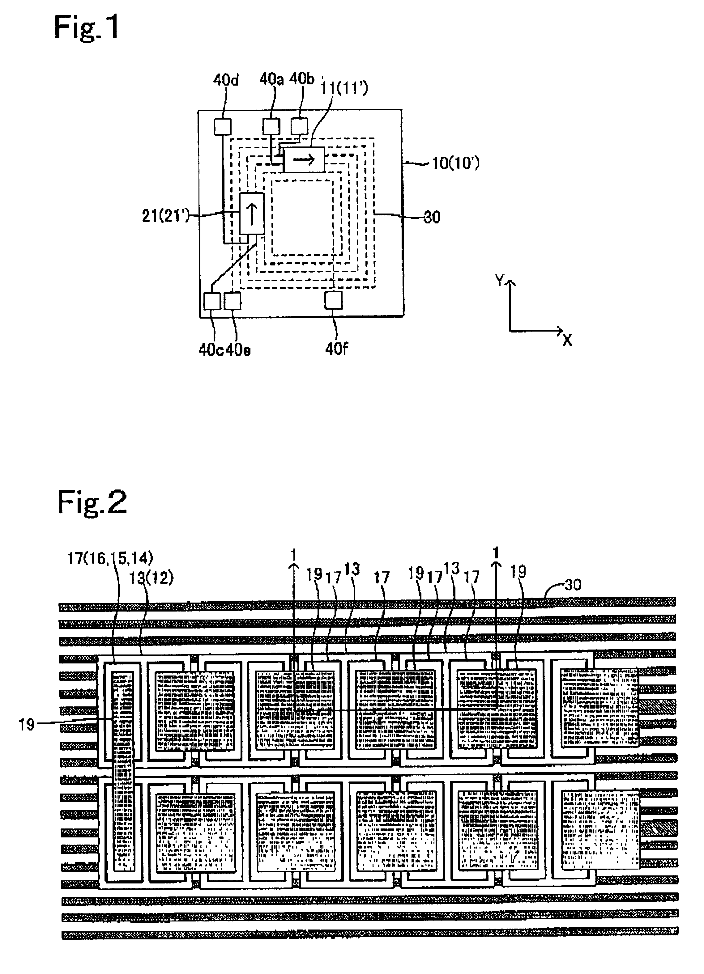
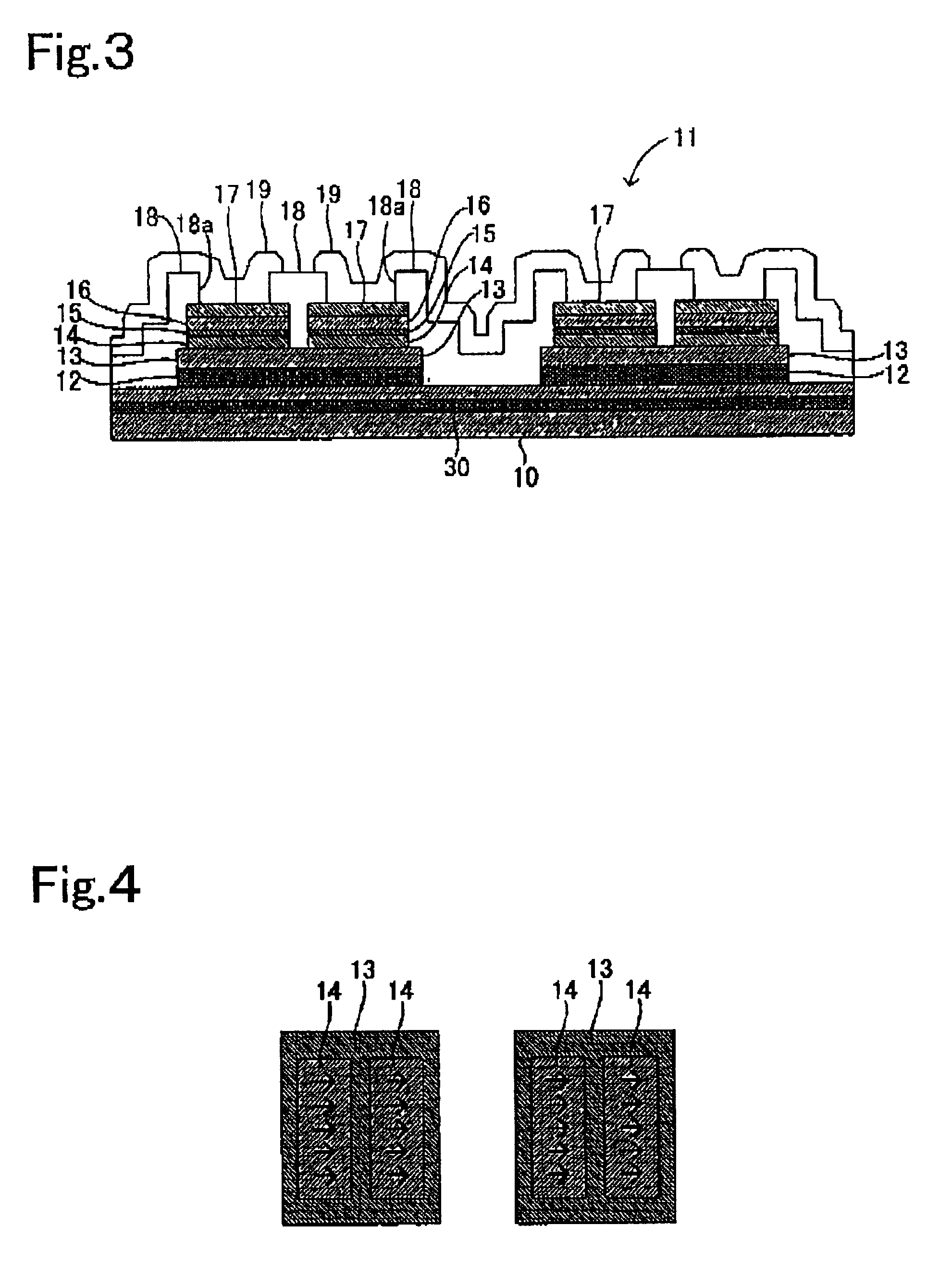
[0073]Hereafter, embodiments of the magnetic sensor according to the present invention will be described with reference to the attached drawings. The magnetic sensor includes a generally square-shaped substrate 10 made of, for example, SiO2 / Si, glass, or quartz, two magnetic tunnel affect elements (groups) 11, 21, a coil 30 for bias magnetic field, and a plurality of electrode pads 40a to 40f, as illustrated in the plan view of FIG. 1. Magnetic tunnel effect elements (groups) 11, 21 and coil 30 for bias magnetic field are connected respectively to electrode pads 40a, 40b, 40c, 40d, and 40e, 40f. Since magnetic tunnel effect element (group) 11 and magnetic tunnel effect element (group) 21 are identical in structure, magnetic tunnel effect element (group) 11 will be described hereafter as a representative example, and the description of magnetic tunnel effect element (group) 21 will be omitted.

[0074]Magnetic tunnel effect element (group) 11 is made of a plurality of (in this example,...

second embodiment

[0094]Namely, in the second embodiment, as illustrated in FIG. 22, a film made of Ta having a thickness of 30 nm, a film made of MnRh having a thickness of 30 nm, and a film made of NiFe having a thickness of 40 nm are formed on a substrate 10 by sputtering so as to form a lower magnetic layer SJ. Subsequently, an Al film of 1 nm is formed and oxidized to form an insulating layer 15. A film made of NiFe having a thickness of 40 nm and a film made of Ta having a thickness of 40 nm are formed thereon so as to form an upper magnetic layer UJ.

[0095]Subsequently, as illustrated In FIG. 23, the upper magnetic layer UJ is processed for separation, and the lower magnetic layer SJ is processed for separation, as illustrated in FIG. 24. Next, as illustrated in FIG. 25, SiO2 is sputtered to form a film having a thickness of 250 nm so as to form an interlayer insulating layer 18, and successively a contact hole 18a is formed through the interlayer insulating layer 18, as illustrated in FIG. 26....

third embodiment

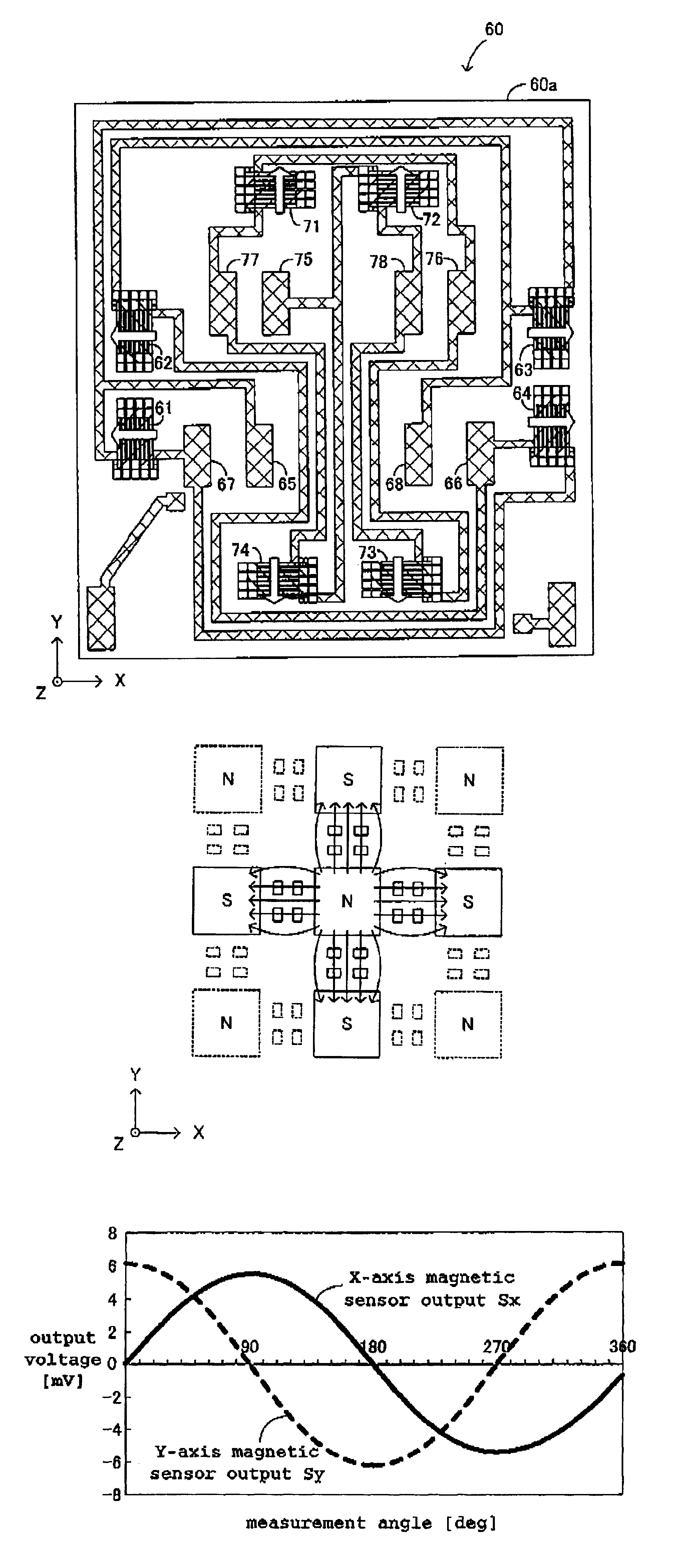
[0126]As described above, a magnet array is prepared which is constructed in such a manner that a plurality of permanent magnets are disposed at lattice points of a square lattice and the polarity of the magnetic pole of each permanent magnet is different from the polarity of the magnetic pole of the other permanent magnets adjacent thereto and spaced apart therefrom by the shortest distance, and the magnetization direction of the magnetic layer that will become the aforesaid pinned layer is pinned with the use of the magnetic fields formed by the magnet array. Therefore, on a single chip, one can easily form GMR elements in which the pinned magnetization directions of the pinned layers are different from each other (perpendicular to each other). Further, by this method, one can produce single chips each having GMR elements in which the pinned magnetization directions of the pinned layers are different from each other, at a time and in a large amount, thereby leading to reduction i...


PUM

PropertyMeasurementUnit
thicknessaaaaaaaaaa
thicknessaaaaaaaaaa
thicknessaaaaaaaaaa

Abstract

On a single chip are formed a plurality of magnetoresistance effect elements provided with pinned layers having fixed magnetization axes in the directions that cross each other. On a substrate 10 are formed magnetic layers that will become two magnetic tunnel effect elements 11, 21 as magnetoresistance effect elements. Magnetic-field-applying magnetic layers made of NiCo are formed to sandwich the magnetic layers in plan view. A magnetic field is applied to the magnetic-field-applying magnetic layers. The magnetic field is removed after the magnetic-field-applying magnetic layers are magnetized in the direction shown by arrow A. As a result of this, by the residual magnetization of the magnetic-field-applying magnetic layers, magnetic fields in the directions shown by arrows B are applied to the magnetic layers that will become magnetic tunnel effect elements 11, 21, whereby the magnetization of the pinned layers of the magnetic layers that will become magnetic tunnel effect elements 11, 21 is pinned in the directions shown by arrows B.

Description

BACKGROUND OF THE INVENTION[0001]1. Field of the Invention[0002]The present invention relates to a magnetic sensor using a magnetoresistance effect (magnetoresistive effect) element containing a pinned layer and a free layer, and more particularly to a magnetic sensor having two or more magnetoresistance effect elements formed on a single chip where the magnetization directions of the pinned layers of the magnetoresistance effect elements cross each other, as well as a method of producing the same.[0003]2. Description of the Background Art[0004]Hitherto, as an element usable in a magnetic sensor, there are known a giant magnetoresistance element (GMR element), a magnetic tunnel effect element (TMR element, tunneling GMR), and others. These magnetoresistance effect elements are provided with a pinned layer whose magnetization direction is pinned (fixed) in a predetermined direction and a free layer whose magnetization direction changes in accordance with an external magnetic field, t...

Claims


Application Information

Patent Timeline
Patent Type & Authority Patents(United States)
IPC IPC(8): G01R33/06G01R33/09H01F41/30H01F41/14H01F10/14H01F41/18H01L43/08H01L43/12
CPCB82Y25/00B82Y40/00G01R33/09H01F41/302G01R33/093Y10T428/32Y10T29/49002Y10T29/49037H10N50/10
Inventor SATO, HIDEKIOOHASHI, TOSHIYUKIWAKUI, YUKIOYOSHIDA, SUSUMUAISO, KOKICHI
Owner YAMAHA CORP
Why Eureka
Try Eureka