Eureka AIR delivers breakthrough ideas for toughest innovation challenges, trusted by R&D personnel around the world.

Semiconductor integrated circuit

Inactive Publication Date: 2005-06-14
KK TOSHIBA
View PDF7 Cites 7 Cited by
  • Summary
  • Abstract
  • Description
  • Claims
  • Application Information

AI Technical Summary

Benefits of technology

[0018]A semiconductor integrated circuit according to an embodiment of the invention comprises: a transistor which has a first electrode, a second electrode and a third electrode, said transistor conducting a current of a first power source from the second electrode to the third electrode by a power supplied to the first electrode; a driver to supply said first electrode with power for driving said transistor; a reference voltage circuit to generate a reference voltage which is variable in response to temperature of said transistor, said reference voltage being used as the reference for comparison; a comparative voltage circuit to generate a comparative voltage which is variable in response to a current flowing from said second electrode to said third electrode, said comparative voltage being compared with said reference voltage; and a controller which receives said reference voltage and said comparative voltage and which supplies a control signal to said driver, said control signal being based on a result of the comparison between the comparative voltage and the reference voltage to control the power supplied to said fir

Problems solved by technology

In general, Semiconductor integrated circuits having a power transistor suffer from heat generated by electric current flowing through the power transistor.
The heat may raise the temperature of the junction of the power transistor, and thereby may break the power transistor and elements placed around it.

Method used


Image

  • Semiconductor integrated circuit
  • Semiconductor integrated circuit
  • Semiconductor integrated circuit

Examples


Embodiment Construction

[0029]Some embodiments of the invention will now be explained below with reference to the drawings. These embodiments, however, should not be construed to limit the invention.

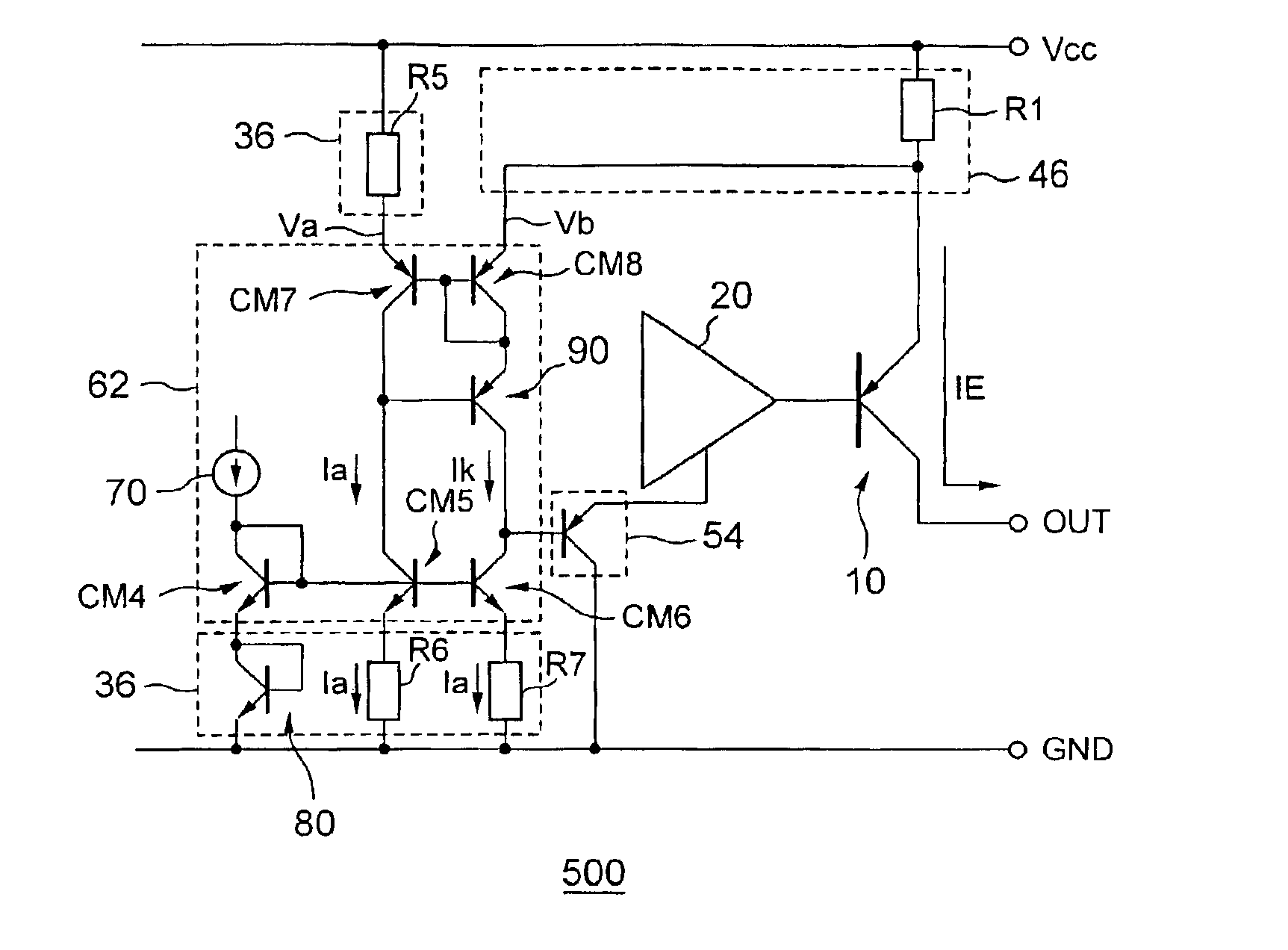
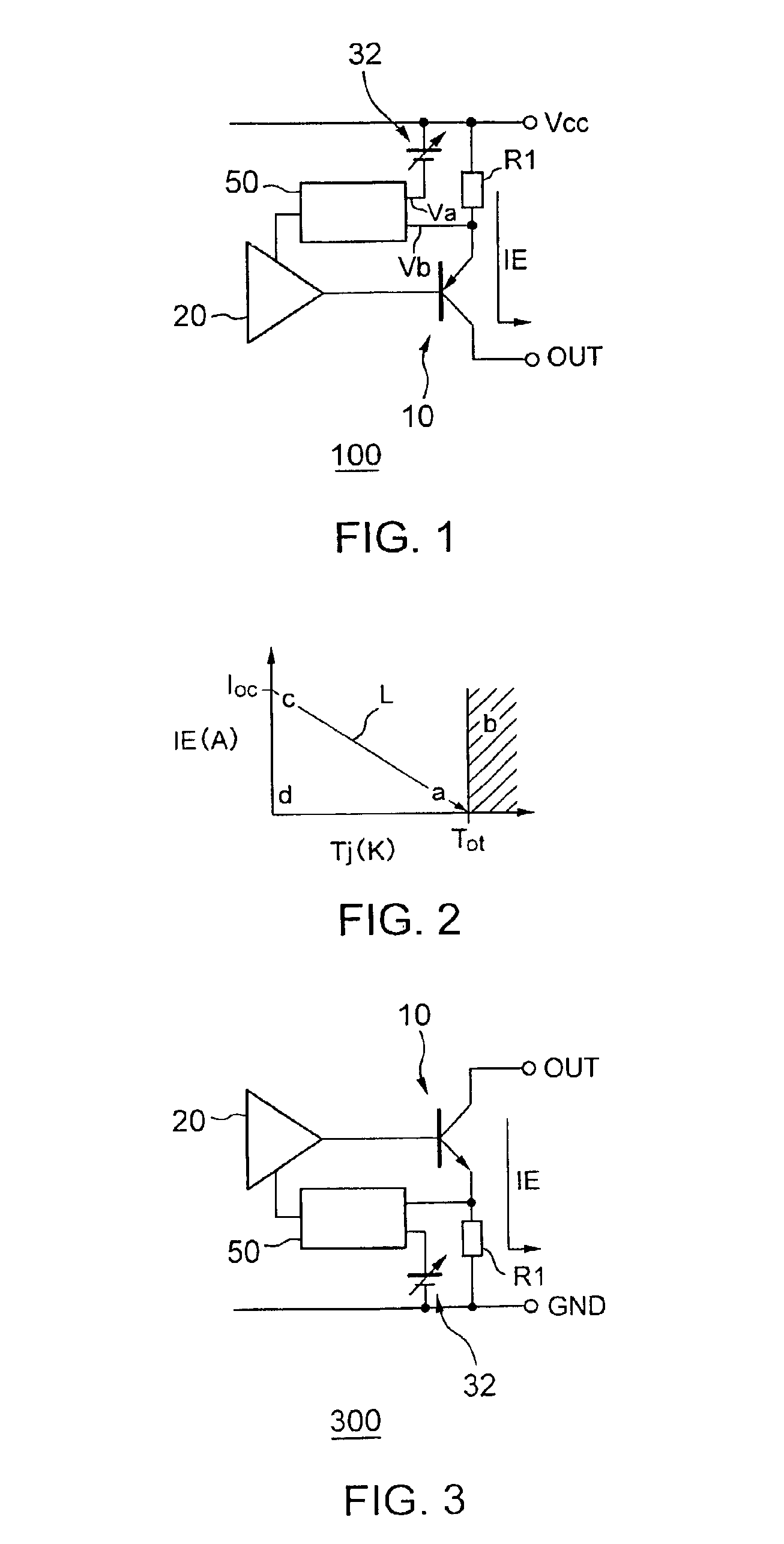
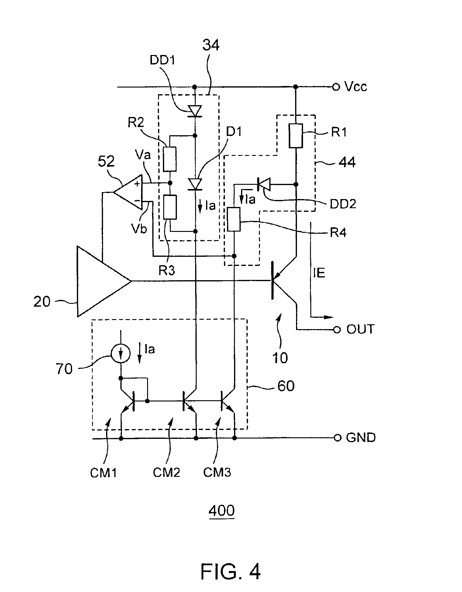
[0030]FIG. 1 is a circuit diagram of a semiconductor integrated circuit 100 according to an embodiment of the invention. The semiconductor integrated circuit 100 includes a bipolar transistor 10 and a driver circuit 20. The bipolar transistor 10 permits a current from a power source VCC to flow from the emitter to the collector as the emitter current IE depending on a current supplied to the base. The driver circuit 20 drives the transistor 10.

[0031]The semiconductor integrated circuit further includes a reference voltage source 32 and a resistor R1. The reference voltage source 32 generates a reference voltage Va variable with temperature Tj of a junction formed inside the transistor 10. The resistor R1 generates a comparative voltage vb compared with the reference voltage Va and variable with the emitter curr...


PUM


Abstract

A semiconductor integrated circuit comprises a transistor which has a first electrode, a second electrode and a third electrode, said transistor conducting a current of a first power source from the second electrode to the third electrode by a power supplied to the first electrode; a driver to supply said first electrode with power for driving said transistor; a reference voltage circuit to generate a reference voltage which is variable in response to temperature of said transistor, said reference voltage being used as the reference for comparison; a comparative voltage circuit to generate a comparative voltage which is variable in response to a current flowing from said second electrode to said third electrode, said comparative voltage being compared with said reference voltage; and a controller which receives said reference voltage and said comparative voltage and which supplies a control signal to said driver, said control signal being based on a result of the comparison between the comparative voltage and the reference voltage to control the power supplied to said first electrode.

Description

CROSS-REFERENCE TO RELATED APPLICATIONS[0001]This application is based upon and claims the benefit of priority from the prior Japanese Patent Application No. 2001-309829, filed on Oct. 5, 2001, the entire contents of which are incorporated herein by reference.BACKGROUND OF THE INVENTION[0002]1. Field of the Invention[0003]This invention relates to a semiconductor integrated circuit.[0004]2. Related Background Art[0005]In general, Semiconductor integrated circuits having a power transistor suffer from heat generated by electric current flowing through the power transistor. The heat may raise the temperature of the junction of the power transistor, and thereby may break the power transistor and elements placed around it.[0006]As a countermeasure, an overheat detector circuit has been provided heretofore to detect the temperature of the junction of the power transistor.[0007]FIG. 8 is a schematic diagram of a conventional semiconductor integrated circuit 800 having an overheat detector...

Claims


Application Information

Patent Timeline
IPC IPC(8): H03K17/082H03K17/08G05F1/56H01L21/822H01L27/04
CPCH03K17/0826Y10S323/907H03K2017/0806
Inventor WATANABE, KIYOMI
Owner KK TOSHIBA
Why Eureka
Eureka Blog
Learn More