Semiconductor integrated circuit and nonvolatile memory element

a technology of integrated circuits and memory elements, applied in semiconductor devices, digital storage, instruments, etc., can solve the problems of large influence on small amount of accumulated charges, and large deterioration of charge retention characteristics, so as to improve the retention capacity of stored information, enhance the ability of long-term data retention, and reduce the rate of readout faults

Inactive Publication Date: 2005-06-14
TESSERA ADVANCED TECH
View PDF23 Cites 24 Cited by
  • Summary
  • Abstract
  • Description
  • Claims
  • Application Information

AI Technical Summary

Benefits of technology

[0018]An object of the present invention is to provide a semiconductor integrated circuit which can remarkably enhance a long-term information retention capability based on a memory cell including a pair of nonvolatile memory elements in a differential form.
[0033]When notice is taken of the fact that the nonvolatile memory elements can be formed using the manufacturing process, such as the single-layer polysilicon process, the floating gates of the MIS transistors constructing the nonvolatile memory elements, the gates of the MIS transistors included in the logic circuit, the gates of the MIS transistors included in the input / output circuit, and the gates of the MIS transistors included in the DRAM may be formed to have equal film thicknesses within the allowable range of errors ascribable to process deviations. That is, even with the single-layer polysilicon process or the like single-layer gate process, it is possible to obtain a semiconductor integrated circuit, such as a system LSI in which a DRAM formed of the nonvolatile memory having an excellent data retention capability, etc. is simultaneously merged and packaged.

Problems solved by technology

It has been found by the inventors that even a memory cell structure in the differential form has a first problem in that the occurring rate of readout faults ascribable to the deterioration of charge retention characteristics are greatly affected by the states of an initial threshold voltage under which no charge exists in a floating gate, threshold voltages in write and erase states, and a word line potential in a readout operation.
That is, the quantity of accumulated charges is small, and a retaining field strength which is applied to a tunnel oxide film in a retention state is low.
As a result, the fall of the threshold voltage attributed to charge leakage from the floating gate is difficult to develop.

Method used


Image

  • Semiconductor integrated circuit and nonvolatile memory element
  • Semiconductor integrated circuit and nonvolatile memory element
  • Semiconductor integrated circuit and nonvolatile memory element

Examples


Embodiment Construction

[System LSI]

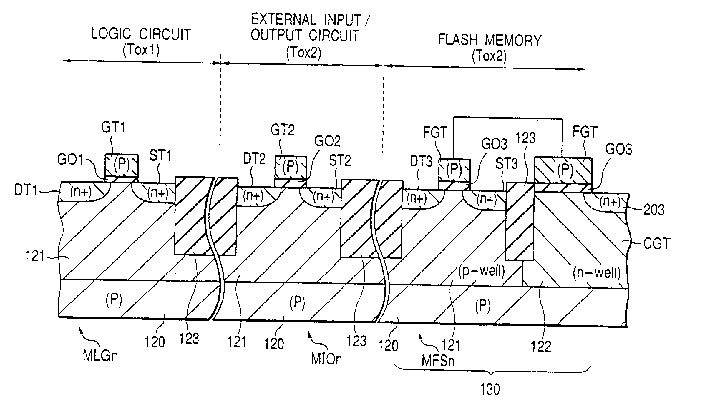
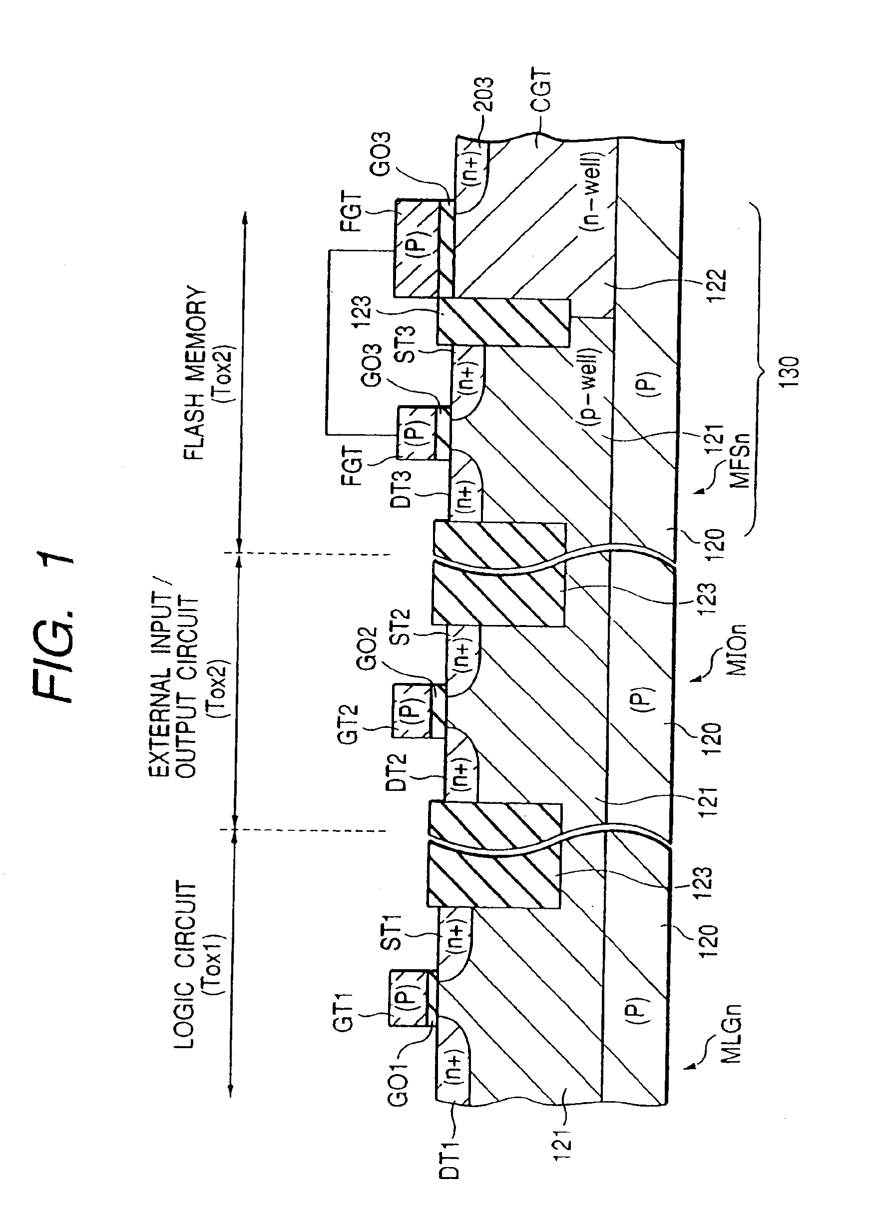
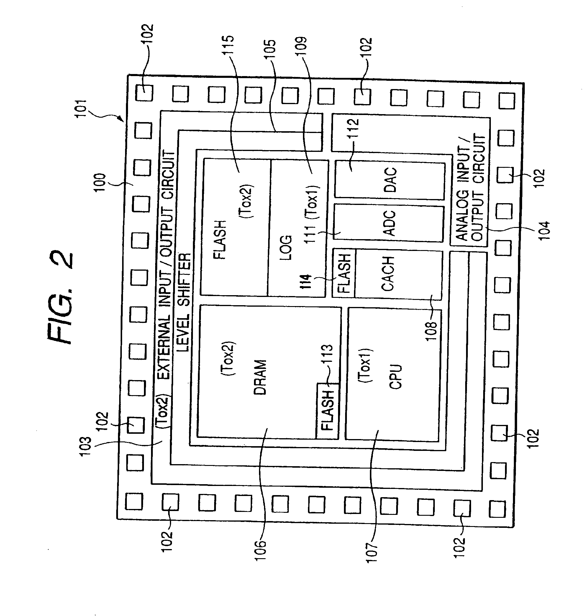
[0068]Schematically shown in FIG. 2 is a chip plan view of a system LSI which represents an example of a semiconductor integrated circuit according to the present invention. Although the invention is not especially restricted thereto, the system LSI 101 illustrated in the figure is so constructed that a large number of external connection electrodes, such as bonding pads, 102 are arranged at the peripheral edge of a semiconductor substrate 100, and that an external input / output circuit 103 and an analog input / output circuit 104 are disposed inside the electrodes 102. The external input / output circuit 103 and the analog input / output circuit 104 have an operating supply voltage which is an external supply voltage of relatively high level, such as 3.3 V. A level shifter 105 steps down the external supply voltage to an internal supply village such as 1.8 V. Inside the level shifter 105, there are a dynamic random access memory (DRAM) 106, a central processing unit (CPU) 107,...


PUM


Abstract

0 Owing to the above, even with the single-layer gate process such as single-layer polysilicon gate process, it is possible to obtain a semiconductor integrated circuit such as system LSI in which a nonvolatile memory which is excellent in data retention capability is merged and packaged with a DRAM etc. Further, since the nonvolatile memory of high reliability can be formed without adding any step to a related art manufacturing process, such as a standard CMOS manufacturing process, the present invention may be readily applied to an LSI in which the nonvolatile memory and a logic LSI, or the nonvolatile memory and a DRAM are merged and packaged on an identical semiconductor substrate. Accordingly, a system LSI in which a flash memory is merged and packaged can be provided without increasing the cost of manufacture.

Description

CROSS-REFERENCE TO RELATED APPLICATION[0001]This application is a continuation of application Ser. No. 10 / 610,567 filed on Jul. 2, 2003, now U.S. Pat. No. 6,771,538, which is a continuation of application Ser. No. 09 / 493,280 filed on Jan. 28, 2000, now U.S. Pat. No. 6,614,684. The contents of application Ser. Nos. 10 / 610,567 and 09 / 493,280 are hereby incorporated herein by reference in their entirety.BACKGROUND OF THE INVENTION[0002]The present invention relates to a semiconductor integrated circuit having electrically erasable and programmable nonvolatile memory elements. More particularly, the invention relates, for example, to techniques which are effective when applied to a semiconductor integrated circuit having a nonvolatile memory wherein two nonvolatile memory elements are used as a storage unit.[0003]In recent years, as a memory device in which data or program-constituting data are stored, substantial public attention has been directed to a flash EEPROM (hereinbelow, termed...

Claims


Application Information

Patent Timeline
Patent Type & Authority Patents(United States)
IPC IPC(8): G11C16/28G11C16/04G11C16/06G11C11/34G11C16/10H01L21/8247H01L27/105
CPCB82Y10/00H01L27/1052G11C16/0416G11C16/0441G11C16/10G11C16/28H01L27/105H01L27/115H01L27/11519H01L27/11521H01L27/11526H01L27/11546H01L27/11558H01L29/66825H01L29/7883G11C16/04G11C16/349G11C2216/08G11C2216/10H10B99/00H10B69/00H10B41/10H10B41/30H10B41/40H10B41/49H10B41/60G11C16/06
Inventor SHUKURI, SHOJIKOMORI, KAZUHIROKUBOTA, KATSUHIKOOKUYAMA, KOUSUKE
Owner TESSERA ADVANCED TECH
Why Eureka
Try Eureka