Method and apparatus for encapsulation of an edge of a substrate during an electro-chemical deposition process

a technology of electrochemical deposition and substrate, which is applied in the direction of sealing devices, coupling device connections, manufacturing tools, etc., can solve the problems of high aspect ratio features, difficult filling structures with copper materials, and inability to achieve uniform plating,

Inactive Publication Date: 2005-06-21
APPLIED MATERIALS INC
View PDF47 Cites 47 Cited by
  • Summary
  • Abstract
  • Description
  • Claims
  • Application Information

AI Technical Summary

Benefits of technology

[0029]To facilitate understanding, identical reference numerals have been used, wherever possible, to designate identical elements that are common to the figures.

Problems solved by technology

However, many traditional deposition processes, such as physical vapor deposition (PVD) and chemical vapor deposition (CVD), have difficulty filling structures with copper material where the aspect ratio exceeds 4:1, and particularly where it exceeds 10:1.
As a result of these process limitations, electroplating, which had previously been limited to the fabrication of lines on circuit boards, is now being used to fill vias and contacts on semiconductor devices.
While present day electroplating cells achieve acceptable results on larger scale substrates, a number of obstacles impair consistent reliable electroplating onto substrates having micron-sized, high aspect ratio features.
For example, the electrical contacts between the substrate and the deposition system are often exposed to the plating fluid (e.g., electrolyte) and subsequently become contaminated with deposition material or other contaminants that reduce the contact area between the substrate and contacts.
The reduced or irregular contact area disrupts uniform biasing of the substrate that results in non-uniform plating.
Moreover, the position of the contacts relative to the center of the substrate may additionally create non-uniform power distribution over the substrate.
Tight tolerance requirements are generally undesirable due to the increase in part, assembly and quality assurance costs.

Method used


Image

  • Method and apparatus for encapsulation of an edge of a substrate during an electro-chemical deposition process
  • Method and apparatus for encapsulation of an edge of a substrate during an electro-chemical deposition process
  • Method and apparatus for encapsulation of an edge of a substrate during an electro-chemical deposition process

Examples


Embodiment Construction

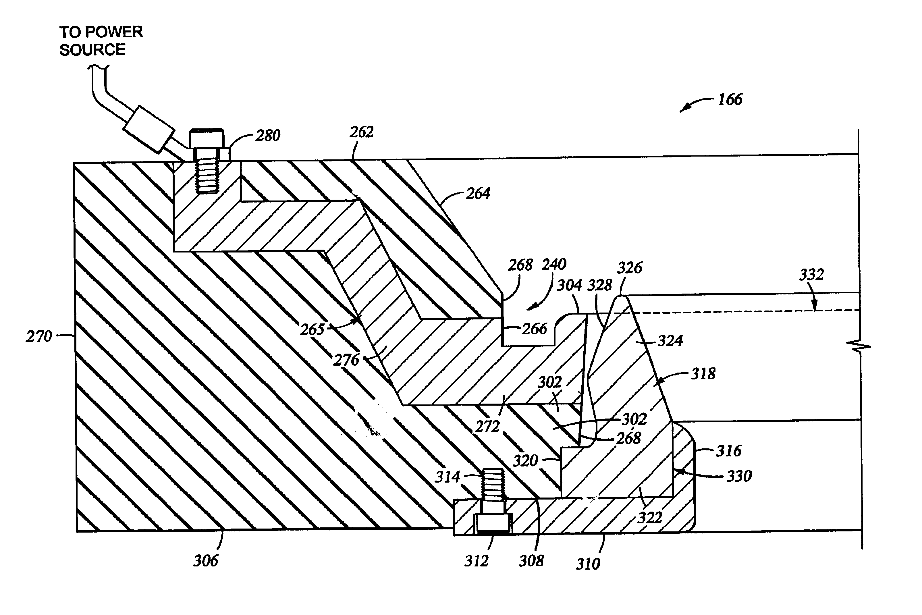
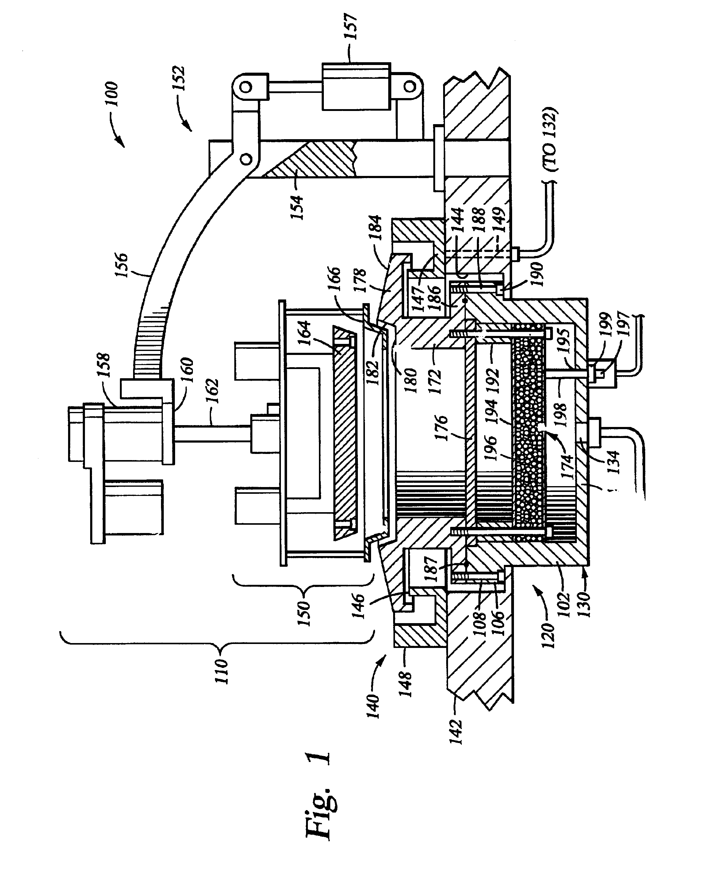
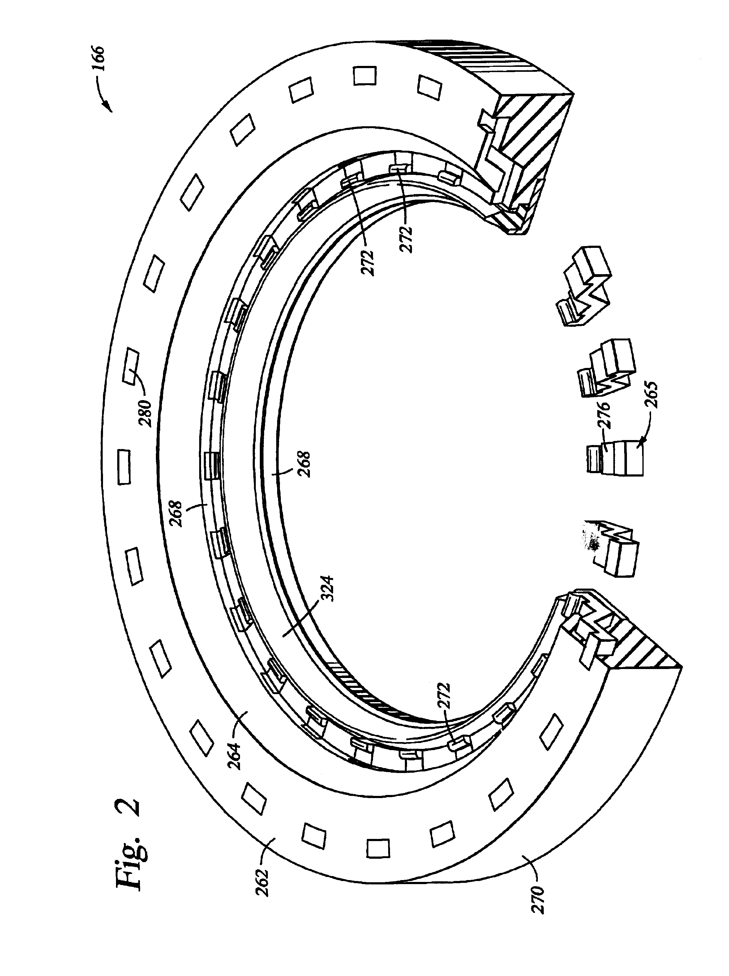
[0030]FIG. 1 is a cross sectional view of an electroplating process cell 100 according to the invention. The processing cell 100 generally comprises a head assembly 110, a process kit 120 and an electrolyte collector 140. Preferably, the electrolyte collector 140 is secured onto the base 142 over an opening 144 that defines the location for placement of the process kit 120. The electrolyte collector 140 includes an inner wall 146, an outer wall 148 and a bottom 147 connecting the walls 147, 148. An electrolyte outlet 149 is disposed through the bottom 147 of the electrolyte collector 140 and connected to an electrolyte replenishing system 132 through tubes, hoses, pipes or other fluid transfer connectors.

[0031]The head assembly 110 is mounted onto a head assembly frame 152. The head assembly frame 152 includes a mounting post 154 and a cantilever arm 156. The mounting post 154 is mounted onto the base 142 of the electroplating process cell 100, and the cantilever arm 156 extends lat...


PUM

PropertyMeasurementUnit
thicknessaaaaaaaaaa
conductiveaaaaaaaaaa
areaaaaaaaaaaa

Abstract

An electro-chemical deposition method and apparatus that encapsulates a substrate's edge to prevent deposition thereon is generally provided. In one embodiment, the apparatus includes a contact ring, one or more electrical contact pads disposed on the contact ring and a thrust plate axially movable relative to the contact ring. A first seal is disposed inward of the contact pad and seals with the contact ring. A second seal is coupled to the thrust plate. The first and second seals are adapted to sandwich the substrate therebetween when the contact ring and the thrust plate are moved towards each other. In another embodiment, a third seal provides a seal between the thrust plate and contact ring, and, with the first and second seals, defines an exclusion zone encapsulating the substrate's edge. One or more electrical contact pads are protected from the electrolyte by being disposed within the exclusion zone.

Description

BACKGROUND OF THE INVENTION[0001]1. Field of the Invention[0002]Embodiments of the invention generally relate to a method and apparatus for electrochemical deposition of a conductive material on a substrate.[0003]2. Background of the Related Art[0004]Sub-quarter micron, multi-level metallization is one of the key technologies for the next generation of ultra large scale integration (ULSI). The multilevel interconnects that lie at the heart of this technology require planarization of interconnect features formed in high aspect ratio apertures, including vias, contacts, lines, plugs and other features. Reliable formation of these interconnect features is very important to the success of ULSI and to the continued effort to increase circuit density and quality on individual substrates and die.[0005]As circuit densities increase, the widths of vias, contacts, lines, plugs and other features, as well as the dielectric materials between them, decrease to less than 250 nanometers, whereas t...

Claims


Application Information

Patent Timeline
Patent Type & Authority Patents(United States)
IPC IPC(8): C25D7/12C25D17/06H01L21/00
CPCC25D7/12C25D17/004H01L21/67126C25D17/06
Inventor KHOLODENKO, ARNOLD
Owner APPLIED MATERIALS INC
Why Eureka
Try Eureka