Method of manufacturing a FeRAM with annealing process

a manufacturing method and feram technology, applied in the direction of capacitors, semiconductor devices, electrical equipment, etc., can solve the problems of inability to write/read ferroelectric capacitors, relative high voltage, etc., to prevent degradation of dielectric films constituting capacitors, improve capacitor characteristics, and improve the effect of capacitor characteristics

Inactive Publication Date: 2005-06-21
FUJITSU SEMICON LTD
View PDF10 Cites 4 Cited by
  • Summary
  • Abstract
  • Description
  • Claims
  • Application Information

AI Technical Summary

Benefits of technology

[0015]It is an object of the present invention to provide a semiconductor device manufacturing method capable of reducing shift of moisture from an insulating film to a capacitor rather than the prior art.
[0020]Therefore, according to the present invention, an amount of moisture shifted from the insulating film to the capacitor by the annealing process executed after the capacitor is formed, e.g., the annealing process applied to improve the capacitor characteristics or the annealing process applied to form other insulating film is reduced, and thus degradation of the dielectric film constituting the capacitor is prevented.

Problems solved by technology

Thus, the relatively high voltage is needed.
By the way, if the reducing substance is present around the ferroelectric film, there is such a possibility that writing / reading of the ferroelectric capacitor cannot be executed since the polarization characteristic of the ferroelectric film is deteriorated.

Method used


Image

  • Method of manufacturing a FeRAM with annealing process
  • Method of manufacturing a FeRAM with annealing process
  • Method of manufacturing a FeRAM with annealing process

Examples


Embodiment Construction

[0030]An embodiment of the present invention will be explained with reference to the drawings hereinafter.

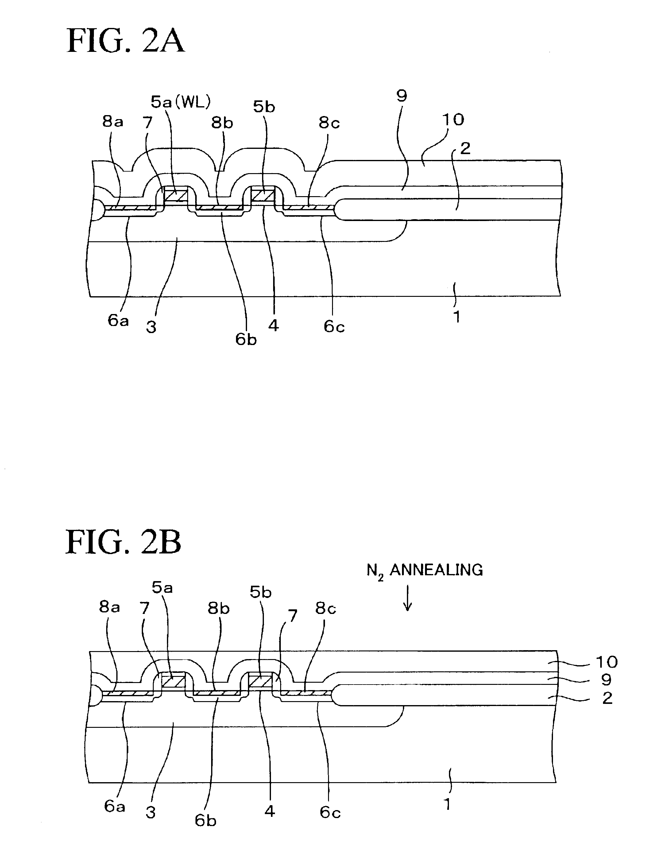
[0031]FIGS. 2A to 2O are sectional views showing a semiconductor device manufacturing method according to an embodiment of the present invention in order of step.

[0032]Next, steps required until a sectional structure shown in FIG. 2A is obtained will be explained hereunder.

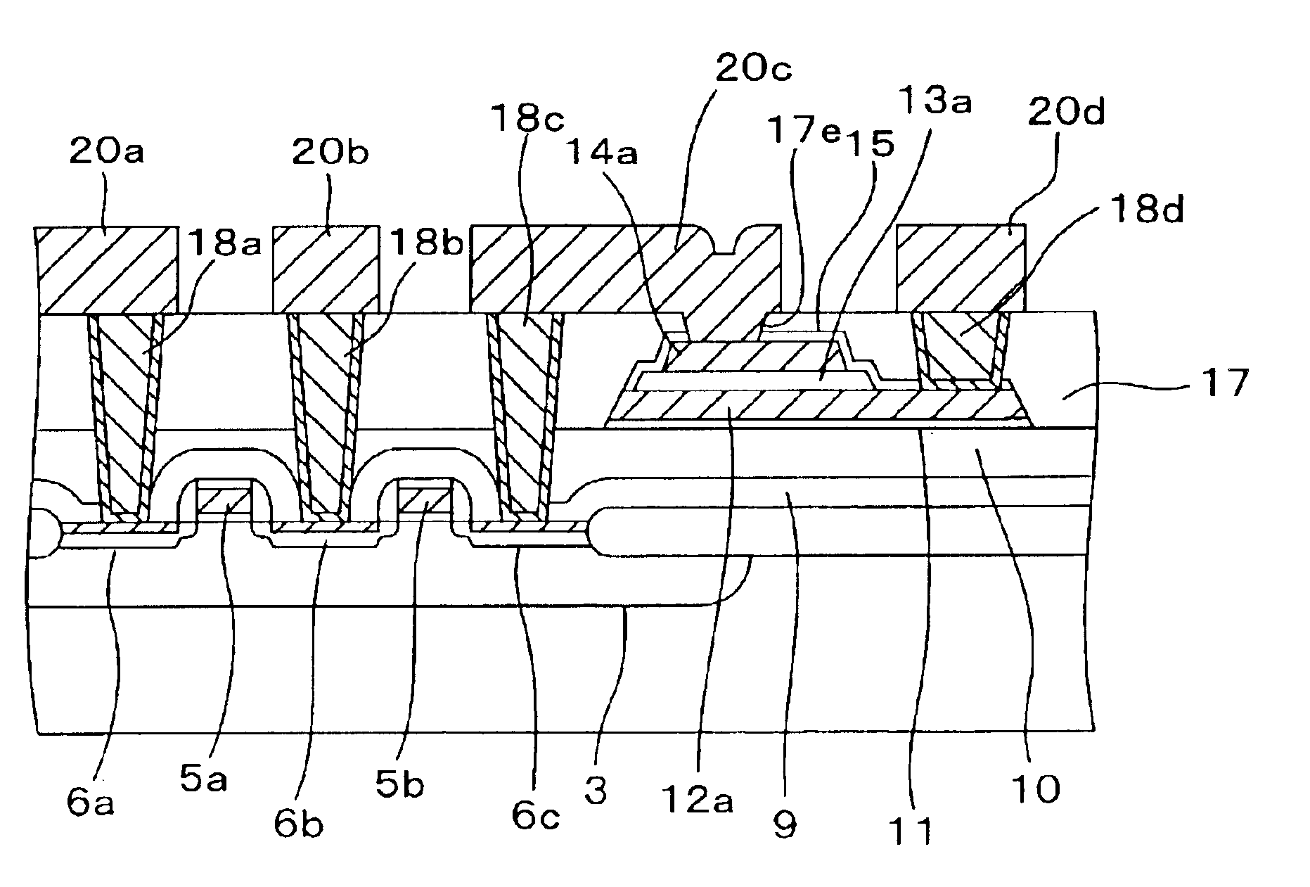
[0033]First, an element isolation insulating film 2 is formed around an active region (transistor forming region) of an n-type or p-type silicon (semiconductor) substrate 1 by the LOCOS (Local Oxidation of Silicon) method. In this case, the STI (Shallow Trench Isolation) structure may be employed as the element isolation insulating film 2.

[0034]Then, a p-well 3 is formed by introducing the p-type impurity into the active region in the memory cell region on the silicon substrate 1. Then, a silicon oxide film is formed as a gate insulating film 4 by thermally oxidizing a surface of the active region on the silic...


PUM

PropertyMeasurementUnit
temperatureaaaaaaaaaa
pressureaaaaaaaaaa
thicknessaaaaaaaaaa

Abstract

There are contained the steps of forming sequentially a first conductive film, a dielectric film, and a second conductive film on a first insulating film, forming an upper electrode of a capacitor by patterning the second conductive film, patterning the dielectric film to leave under the upper electrode, forming a lower electrode of the capacitor by patterning the first conductive film, covering the capacitor and the first insulating film with a second insulating film, and annealing at least one of the first insulating film and the second insulating film in an inert-gas atmosphere and then exposing the film to an N2O plasma.

Description

CROSS-REFERENCE TO RELATED APPLICATIONS[0001]This application is based upon and claims priority of Japanese Patent Application No. 2002-180602, filed on Jun. 20, 2002, the contents being incorporated herein by reference.BACKGROUND OF THE INVENTION[0002]1. Field of the Invention[0003]The present invention relates to a semiconductor device manufacturing method and, more particularly, a semiconductor device manufacturing method having a capacitor.[0004]2. Description of the Prior Art[0005]As the nonvolatile memory that can store information after the power supply is turned OFF, the flash memory or the ferroelectric memory (FeRAM) has been known.[0006]The flash memory has the floating gate buried in the gate insulating film of the insulated-gate field effect transistor (IGFET), and stores information by accumulating the charge as stored information in the floating gate. The tunnel current must be passed through the gate insulating film to write / erase the information. Thus, the relativel...

Claims


Application Information

Patent Timeline
Patent Type & Authority Patents(United States)
IPC IPC(8): H01L21/02H01L21/314H01L27/105H01L21/8246H01L27/115
CPCH01L21/3144H01L28/40H01L27/11507H01L27/11502H10B53/30H10B53/00H01L21/0234H01L21/02337
Inventor YOKOTA, TATSUYA
Owner FUJITSU SEMICON LTD
Why Eureka
Try Eureka