Structure of quantum dot light emitting diode and method of fabricating the same

a light-emitting diode and quantum dot technology, applied in the field of structure, can solve the problems of high cost of changing the source system of the original epitaxial apparatus, the modification of the epitaxial apparatus, etc., and achieve the effect of enhancing the probability of recombination of electrons, reducing the mobility of carriers, and reducing the cost of modification

Active Publication Date: 2005-06-21
NAT CHUNG SHAN INST SCI & TECH
View PDF3 Cites 8 Cited by
  • Summary
  • Abstract
  • Description
  • Claims
  • Application Information

AI Technical Summary

Benefits of technology

[0006]An InAs/GaAs quantum dot light emitting diode is disclosed. InAs/GaAs quantum dot light emitting diode which is formed by turning off an As shutter and using As background concentration for epitaxy, comprises a Si-doped GaAs substrate, a N-type structure, an undoped quantum well, ...

Problems solved by technology

The modification of the epitaxial apparatus, however, costs a lot...

Method used


Image

  • Structure of quantum dot light emitting diode and method of fabricating the same
  • Structure of quantum dot light emitting diode and method of fabricating the same
  • Structure of quantum dot light emitting diode and method of fabricating the same

Examples


Embodiment Construction

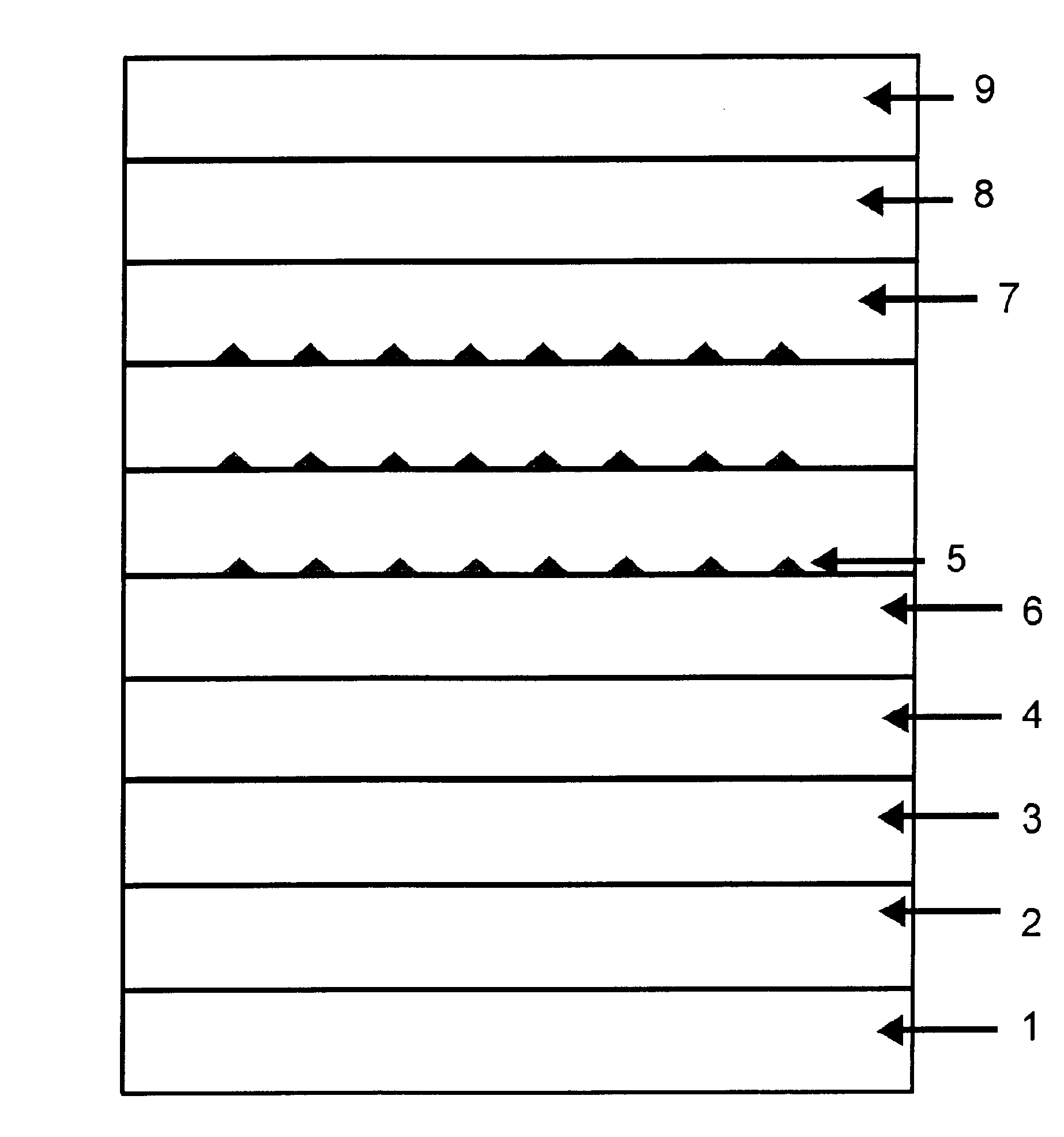
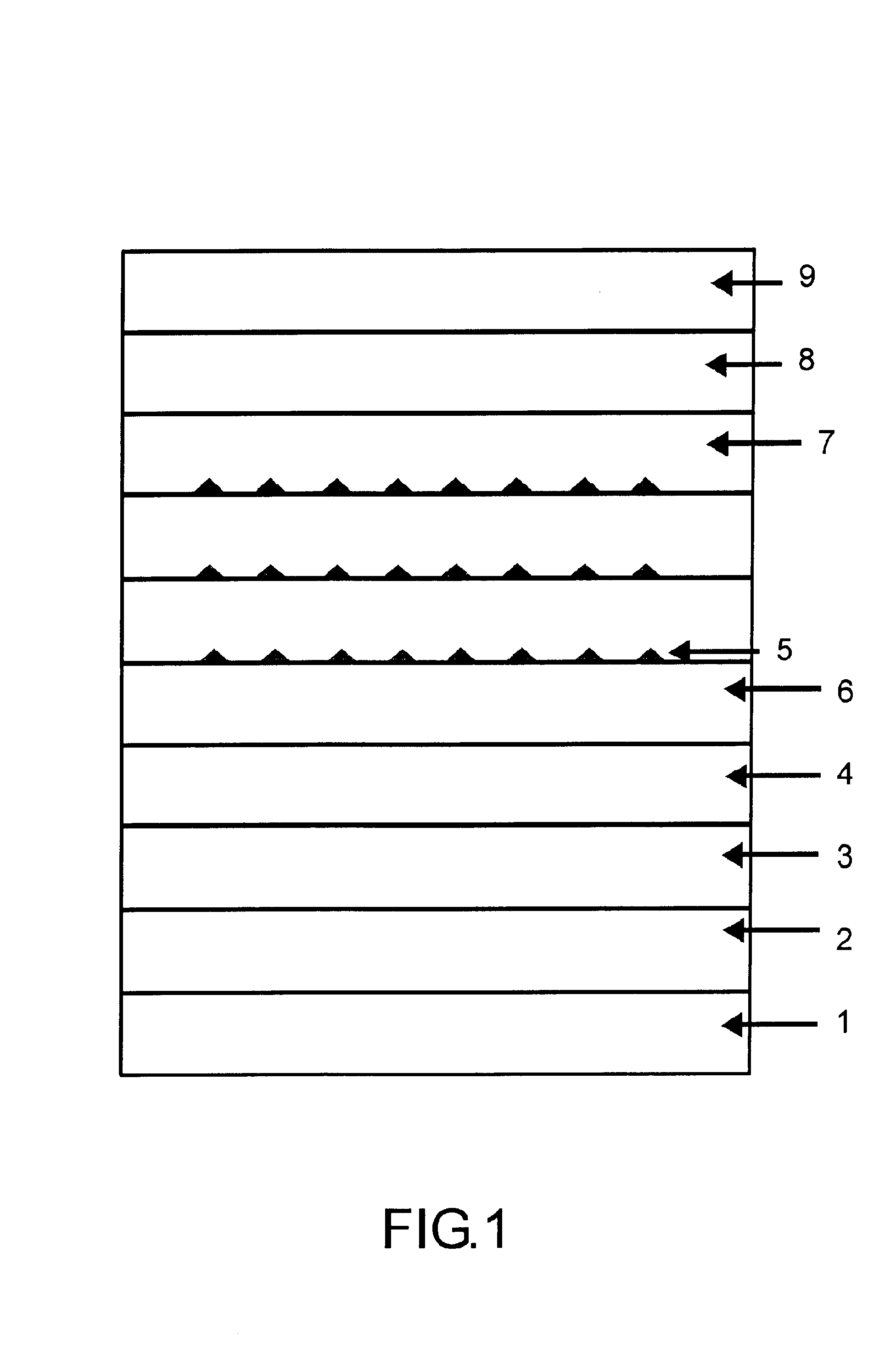
[0010]FIG. 1 is a schematic drawing for showing an epitaxial structure.

[0011]Please referring to FIG. 1, a (001)±1° Si-doped GaAs substrate 1, which has a thickness about from 320 μm to about 380 μm and dopant concentration from about 1×10¹⁸ to about 1×1019 cm−3 is provided. A GaAs buffer layer 2 having a thickness about from 500 nm to about 2000 nm and dopant concentration from about 1×10¹⁸ to about 5×1019 cm−3 is formed on the substrate 1 when substrate temperature is about from 580 to about 615° C. Then, a Al xGa1−xAs cap layer 3 having a thickness about from 200 nm to about 800 nm and dopant concentration from about 1×10¹⁸ to about 5×1018 cm−3 is formed on the GaAs buffer layer 2, wherein x is about 0.3-0.7 when substrate temperature is raised to 610° C. to about 650° C. Two to ten multi-layer GaAs / undoped AlxGa1−xAs quantum wells 4 then are formed on the cap layer 3, wherein each quantum well has a thickness about from 3 nm to about 7 nm, and x is about 0.3-0.7 when substrate t...


PUM


Abstract

An InAs/GaAs quantum dot light emitting diode and a method of fabricating the same are disclosed. The InAs/GaAs quantum dot light emitting diode which is formed by turning off an As shutter and using As background concentration for epitaxy, comprises a Si-doped GaAs substrate, a N-type structure, an undoped quantum well, aseries of quantum dot layers, spacer layers, a barrier layer and a P-type structure.

Description

CROSS REFERENCE TO RELATED APPLICATIONS[0001]This application claims the priority benefit of Taiwan application Ser. No. 92105988, filed on Mar. 19, 2003.BACKGROUND OF INVENTION[0002]1. Field of the Invention[0003]The present invention relates to a structure of InAs / GaAs quantum dot light emitting diode and a method of fabricating the same, and more particularly to a structure of nano-technology light emitting diode and a method of fabricating the same that can improve sensitivity thereof.[0004]2. Description of the Related Art[0005]Traditionally, the method of forming epitaxial structure is performed by a self-organized mold. Because of difference of material surface energy, the energy creates stress thereon, and the material tends to form a low-dimension crystal shape, such as an island. If a new structure is to be formed, the material property can be applied in the method for forming the structure. In some structures, the periodic variations on the surface of the material, a grai...

Claims


Application Information

Patent Timeline
IPC IPC(8): H01L29/02H01L29/12H01L33/00H01L33/02H01L33/06H01L33/30
CPCB82Y10/00H01L29/127H01L33/06H01L33/30Y10S977/95H01L33/02
Inventor TANG, SHIANG-FENGLIN, SHIH-YENLEE, SI-CHENCHERNG, YA-TUNG
Owner NAT CHUNG SHAN INST SCI & TECH
Why Eureka
Try Eureka