Dual panel-type organic electroluminescent display device and method of fabricating the same

Active Publication Date: 2005-06-21
LG DISPLAY CO LTD
View PDF2 Cites 9 Cited by
  • Summary
  • Abstract
  • Description
  • Claims
  • Application Information

AI Technical Summary

Benefits of technology

[0025]An object of the present invention is to provide a dual panel-type organic electroluminescent display device that has improved production yield, high image resolution, and high aperture ratio.
[0026]Another object of the present invention is to provide a method of fabricating a dual panel-type organic electroluminescent display device that has improved production yield, high image resolution, and high aperture ratio.
[0027

Problems solved by technology

However, since passive matrix-type OELD devices have limited resolution, high power consumption, and reduced operational lifetime, active matrix-type OELD devices have been developed as next generation display devices that require high resolution and large display area.
Thus, since supplied voltage and current increase as the total number of the scanning lines increases, the passive matrix-type OELD devices are not adequate to display high resolution images over a large display area due to the high power consumption.
Since the production yield of the array elements multiplied by the production yield of the organic EL diode determines the production yield of the organic EL device,

Method used


Image

  • Dual panel-type organic electroluminescent display device and method of fabricating the same
  • Dual panel-type organic electroluminescent display device and method of fabricating the same
  • Dual panel-type organic electroluminescent display device and method of fabricating the same

Examples


Example

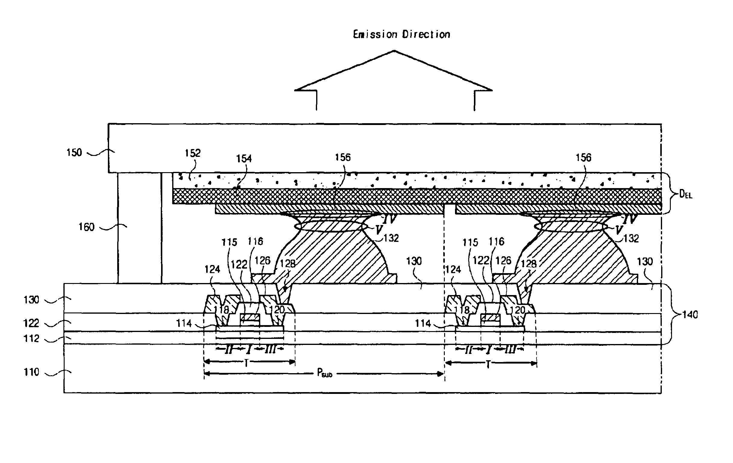
[0042]Reference will now be made in detail to the preferred embodiments of the present invention, examples of which are illustrated in the accompanying drawings.

[0043]FIG. 5 is a schematic cross sectional view of an exemplary organic electroluminescent display device according to the present invention. In FIG. 5, first and second substrates 110 and 150 may be provided to face and be spaced apart from each other, wherein the first and second substrates 110 and 150 may have a plurality of sub-pixel regions “Psub.” In addition, an array element layer 140 including a thin film transistor (TFT) “T” may be formed on an inner surface of the first substrate 110 at each sub-pixel region “Psub.” Although not shown, the array element layer 140 may include a gate line, a data line, a power line, and a common line. Furthermore, a connection pattern 132 of a cylindrical shape may be formed on and connected to the TFT “T” of the array elements 140.

[0044]A first electrode 152 and an organic electro...


PUM


Abstract

An organic electroluminescent display device includes first and second substrates facing and spaced apart from each other, the first and second substrates having a plurality of sub-pixel regions, a thin film transistor provided at each of the plurality of sub-pixel regions on an inner surface of the first substrate, a first electrode on an inner surface of the second substrate, an organic electroluminescent layer on the first electrode, a second electrode on the organic electroluminescent layer at each of the plurality of sub-pixel regions, and a connection pattern contacting the thin film transistor and the second electrode, wherein a melting temperature of the connection pattern is lower than a melting temperature of the second electrode.

Description

[0001]The present invention claims the benefit of Korean Patent Application No. 2002-41938 filed in Korea on Jul. 18, 2002, which is hereby incorporated by reference.BACKGROUND OF THE INVENTION[0002]1. Field of the Invention[0003]The present invention relates to an organic electroluminescent display device and a method of fabricating an organic electroluminescent display device, and more particularly, to a dual panel-type organic electroluminescent device and a method of fabricating a dual panel-type organic electroluminescent display device.[0004]2. Discussion of the Related Art[0005]Among various different types of flat panel display (FPD) devices, organic electroluminescent display (OELD) devices have been developed because of their light-emitting properties, wide viewing angles, and good contrast ratios, as compared with the liquid crystal display (LCD) devices. Since a backlight device is not necessary in the OELD devices, the OELD devices can be light weight and thin. In addit...

Claims


Application Information

Patent Timeline
IPC IPC(8): H01L21/00H01L35/12H01L35/24H05B33/00H01J1/62H01J63/04H01L27/32H01L29/04H01L29/08H01L29/24H01L31/036H01L31/0376H01L31/20H01L33/00H01L51/00H01L51/40H01L51/52H05B33/10H05B33/14
CPCH01L27/3246H01L27/3253H01L51/0024H01L51/5206H01L2251/5315H01L51/0021H10K59/1275H10K59/122H10K71/50H10K71/60H10K50/81H10K2102/3026H05B33/00
Inventor PARK, JAE-YONGYOO, CHOONG-KEUNKIM, OCK-HEELEE, NAM-YANGKIM, KWAN-SOO
Owner LG DISPLAY CO LTD
Why Eureka
Try Eureka