Piezoelectric on semiconductor-on-insulator microelectromechanical resonators

a microelectromechanical and semiconductor technology, applied in piezoelectric/electrostrictive devices, piezoelectric/electrostrictive/magnetostrictive devices, piezoelectric/electrostrictive/magnetostriction machines, etc., can solve the problems of low quality factor of fbar resonators, no electrostatic fine tuning capability, and limited size and cost of frequency selective units in miniature radios and wristwatches

Inactive Publication Date: 2005-06-21
GEORGIA TECH RES CORP
View PDF47 Cites 195 Cited by
  • Summary
  • Abstract
  • Description
  • Claims
  • Application Information

AI Technical Summary

Problems solved by technology

Advanced consumer electronics such as miniature radios and wristwatch cellular phones pose severe limitations on the size and cost of frequency selective units contained therein.
However to reduce the motional resistance of such capacitive resonators for higher frequency applications, gap spacing on the order of nanometer dimensions are often required, which can complicate the fabrication process for these devices.
However, FBAR resonators generally have low quality factors and no electrostatic fine-tuning capabilities.
Further, fabrication methods for these devices are limited practically in their ability to create thick and / or uniform mechanical layers due in part to the long processing times associated with fabrication of thick substrates.

Method used


Image

  • Piezoelectric on semiconductor-on-insulator microelectromechanical resonators
  • Piezoelectric on semiconductor-on-insulator microelectromechanical resonators
  • Piezoelectric on semiconductor-on-insulator microelectromechanical resonators

Examples


first embodiment

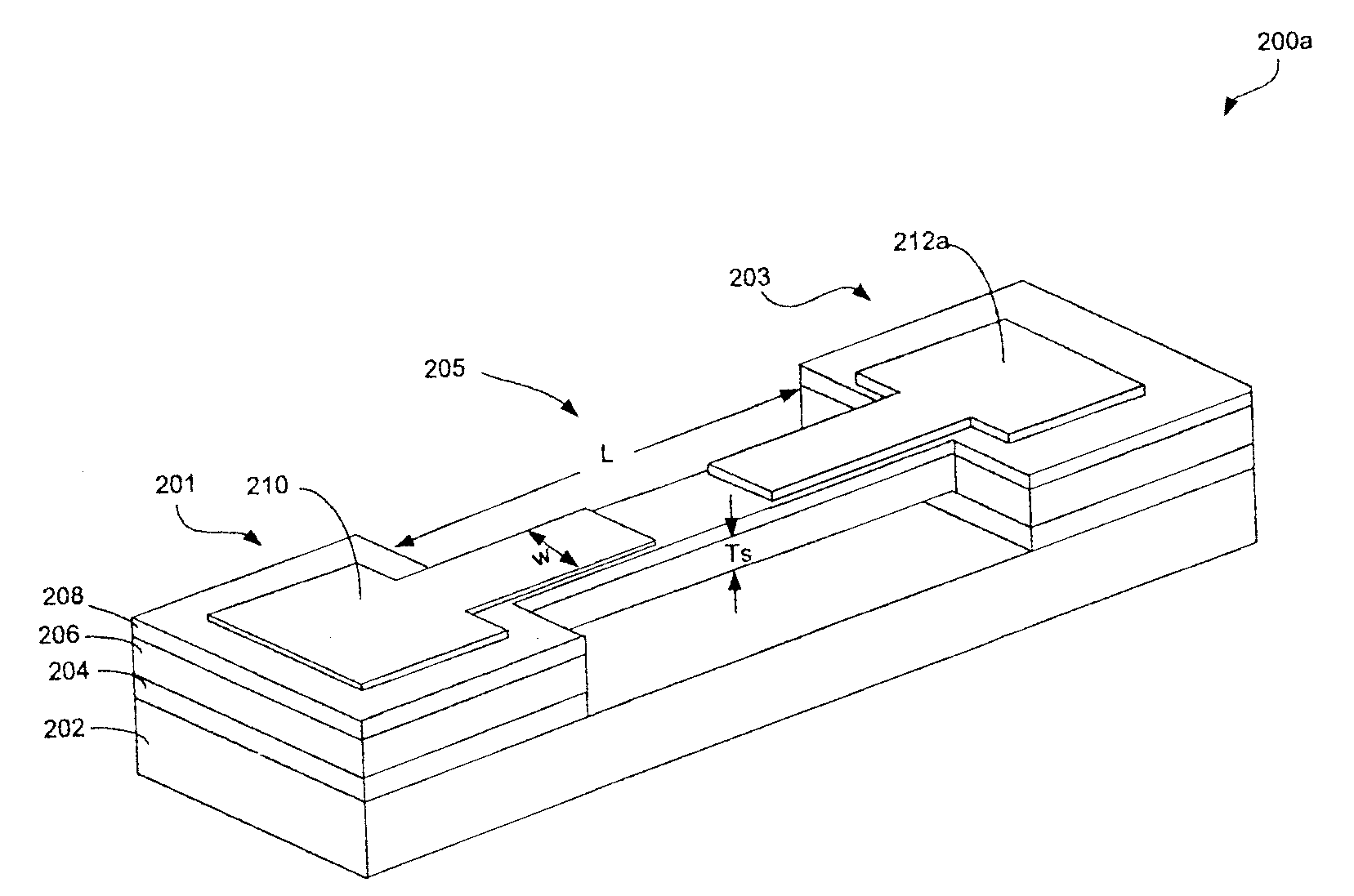
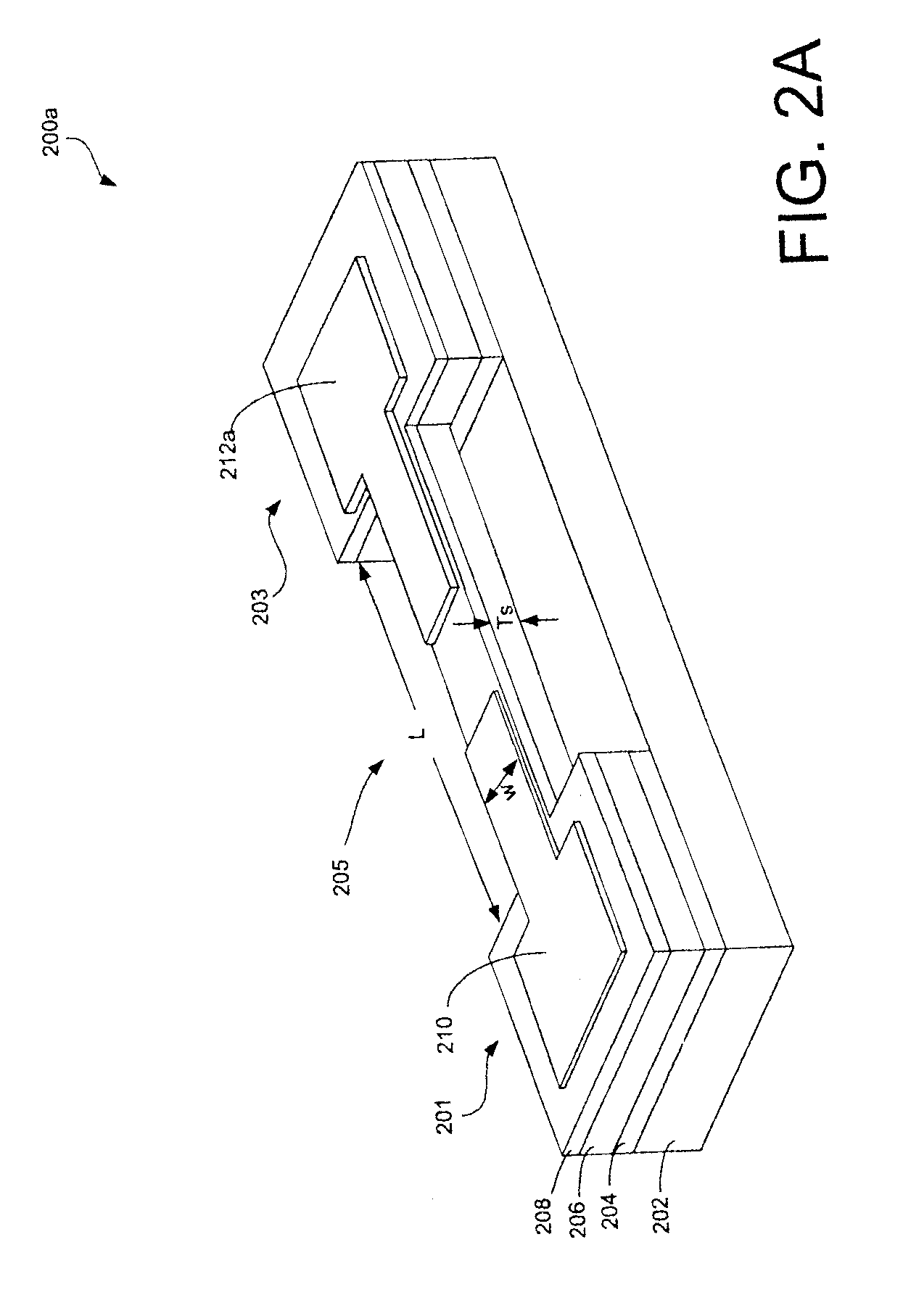
[0025]FIGS. 2A-2C are schematic diagrams that illustrate several piezoelectric beam resonator embodiments. FIG. 2A is a schematic diagram of a first embodiment configured as a clamped-clamped resonator beam 200a. The clamped-clamped resonator beam 200a includes a handle layer 202, an oxide layer 204, a device layer 206, a piezoelectric layer 208, a drive electrode 210, and a sense electrode 212 a The “clamped” regions 201 and 203 correspond to the location where the SOI substrate is secured to the underlying handle layer 202, which in turn can be secured to a printed circuit board, among other devices. In some embodiments, the underlying handle layer 202 is the substrate in an integrated circuit, to which the SOI portion is secured. The “beam” region 205, having a length “L,” spans between the two clamped regions 201 and 203, and includes the portion of the piezoelectric resonator 200a that is free to vibrate. The device layer 206 and the oxide layer 204 collectively represent the S...

second embodiment

[0028]FIG. 2B is a schematic diagram of a second embodiment configured as a clamped-clamped resonator beam 200b with the piezoelectric layer 208 etched away. Layers similar to 202-206 and electrodes 210 and 212a of FIG. 2A are the same as shown in FIG. 2B and thus are not discussed here for clarity. The piezoelectric layer 208 is etched in approximately the middle span of the beam 205 to reduce the effective covering of the beam 205 by the piezoelectric layer 208, thus exposing a surface of the device layer 206. Reducing the effective covering of the beam 205 by the piezoelectric layer 208 can enhance the mechanical Q of the piezoelectric beam resonator 200b (e.g., experimentally proven to at least double the mechanical Q when compared to the embodiment illustrated in FIG. 2A).

third embodiment

[0029]FIG. 2C is a schematic diagram of a third embodiment configured as a clamped-clamped resonator beam 200c with a sensing electrode 212b that extends further along the beam 205 than the sensing electrode 212a of FIGS. 2A-2B. The extending of the sensing electrode 212b covers the area where the strains have the same sign, thus maximizing the sensed strains and providing for improved sensing capability. The sensing electrode 212b extends over the middle span of the beam 205, with the edges located at the inflection points of the beam mode shape. The sensing electrode 212b may cover approximately twice the area covered by the sensing electrode 212a.

[0030]FIG. 3 is a schematic diagram that illustrates another embodiment in the form of a piezoelectric block resonator 300. The piezoelectric block resonator 300 includes a handle layer 302, an oxide layer 304, a device layer 306, a piezoelectric layer 308, a drive electrode 310, and a sense electrode 312. As shown, the piezoelectric bl...


PUM


Abstract

A piezoelectric resonator is disclosed. In one embodiment the piezoelectric resonator includes a resonating member having a bi-directionally adjustable resonance frequency, the resonating member including a semiconductor material of a semiconductor-on-insulator wafer, the semiconductor-on-insulator wafer including an oxide layer adjacent to the semiconductor material and a handle layer adjacent to the oxide layer, the oxide layer disposed between the handle layer and the semiconductor material, and electrode, and a piezoelectric material disposed between the semiconductor material and the electrode, and a capacitor created by the semiconductor material and the handle layer separated by an air gap formed out of the oxide layer, wherein the capacitor is configured to receive a direct current voltage that adjusts the resonance frequency of the resonating member.

Description

CROSS-REFERENCE TO RELATED APPLICATION[0001]This application claims the benefit of U.S. Provisional Application No. 60 / 400,030, filed Aug. 1, 2002, which is entirely incorporated herein by reference.[0002]This application is related to copending U.S. Utility patent application entitled “Capacitive Resonators and Methods of Fabrication,” Ser. No. 10 / 632,176, filed on the same date.STATEMENT REGARDING FEDERALLY SPONSORED RESEARCH OR DEVELOPMENT[0003]The U.S. government has a paid-up license in this invention and the right in limited circumstances to require the patent owner to license others on reasonable terms as provided for by the terms of Contract No. DAAH01-01-1-R004 awarded by the U.S. Army.TECHNICAL FIELD[0004]The present invention is generally related to MEMS (micro-electro-mechanical systems) technology, and, more particularly, is related to piezoelectric resonators.BACKGROUND OF THE INVENTION[0005]Advanced consumer electronics such as miniature radios and wristwatch cellular...

Claims


Application Information

Patent Timeline
Patent Type & Authority Patents(United States)
IPC IPC(8): H03H3/02H03H9/02H03H3/00
CPCH03H3/02H03H2009/02196H03H2003/027
Inventor AYAZI, FARROKHPIAZZA, GIANLUCAABDOLVAND, REZAHO, GAVIN KAR-FAIHUMAD, SHWETA
Owner GEORGIA TECH RES CORP
Why Eureka
Try Eureka