Method and system for monitoring a semiconductor device manufacturing process

a semiconductor device and manufacturing process technology, applied in the field of method and system for monitoring a semiconductor device manufacturing process, can solve the problems of inability to obtain desired shape, inability to avoid changes in pattern shape caused by these variations, and difficulty in high-precision shape checking, etc., and achieve the effect of precise alterations of processing condition parameters

Inactive Publication Date: 2005-06-21
HITACHI LTD
View PDF6 Cites 51 Cited by
  • Summary
  • Abstract
  • Description
  • Claims
  • Application Information

AI Technical Summary

Benefits of technology

[0022]The present invention provides a system for monitoring a semiconductor device manufacturing process that can monitor three dimensional (3-

Problems solved by technology

Moreover, it is difficult to check the shape with high precision, and so a shape check is carried out by cross-sectional observation in most cases.
Even when processing conditions are fixed by the determined condition, it is often the case that a desired shape cannot be obtained due to drift in the property of the equipment etc.
However, since the process is affected by a lot of parameters, as described above, a change in the pattern shape caused by these variations cannot be avoided.
However, among conventional processes, there is no effective means of quantitatively evaluating the slope angle, the shape of a corner part, etc. of the pattern, as shown in FIG. 5, in an invasive manner.
(1) There are cases where an abnormality in the shape of the pattern cannot be detected with dimension values alone.
(2) There are cases where the countervailing measures taken against the formation of a shape abnormality in the pattern cannot be devised with the dimension values alone.
(3) Information that indicates the process variations quantitatively and that is required to monitor the lithography proce

Method used


Image

  • Method and system for monitoring a semiconductor device manufacturing process
  • Method and system for monitoring a semiconductor device manufacturing process
  • Method and system for monitoring a semiconductor device manufacturing process

Examples


first embodiment

(1-0) Fundamental form of Photo Process

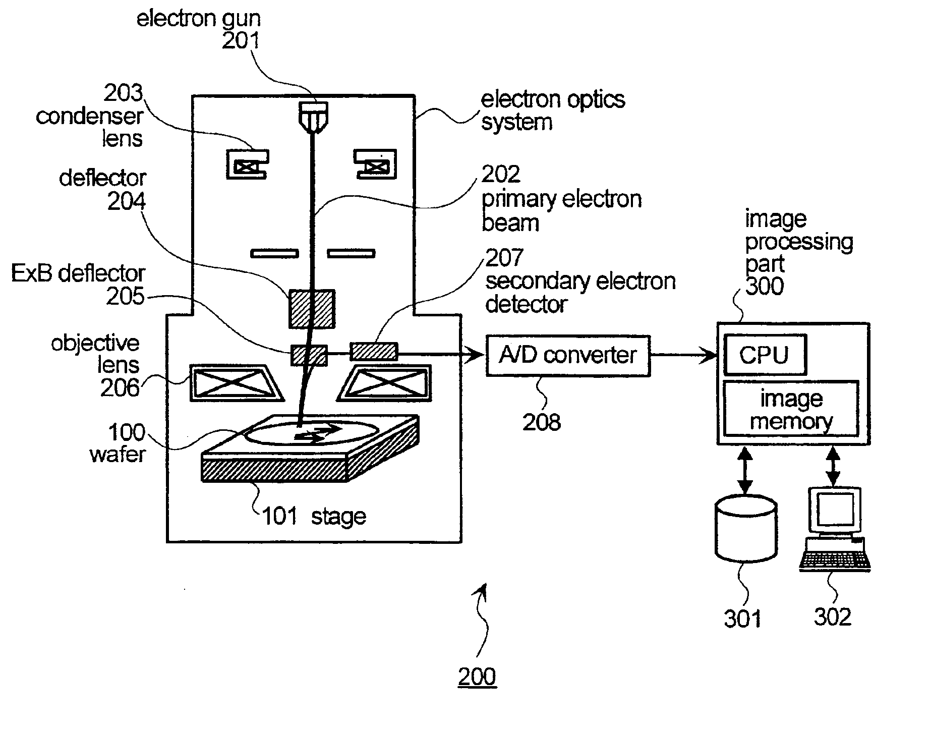
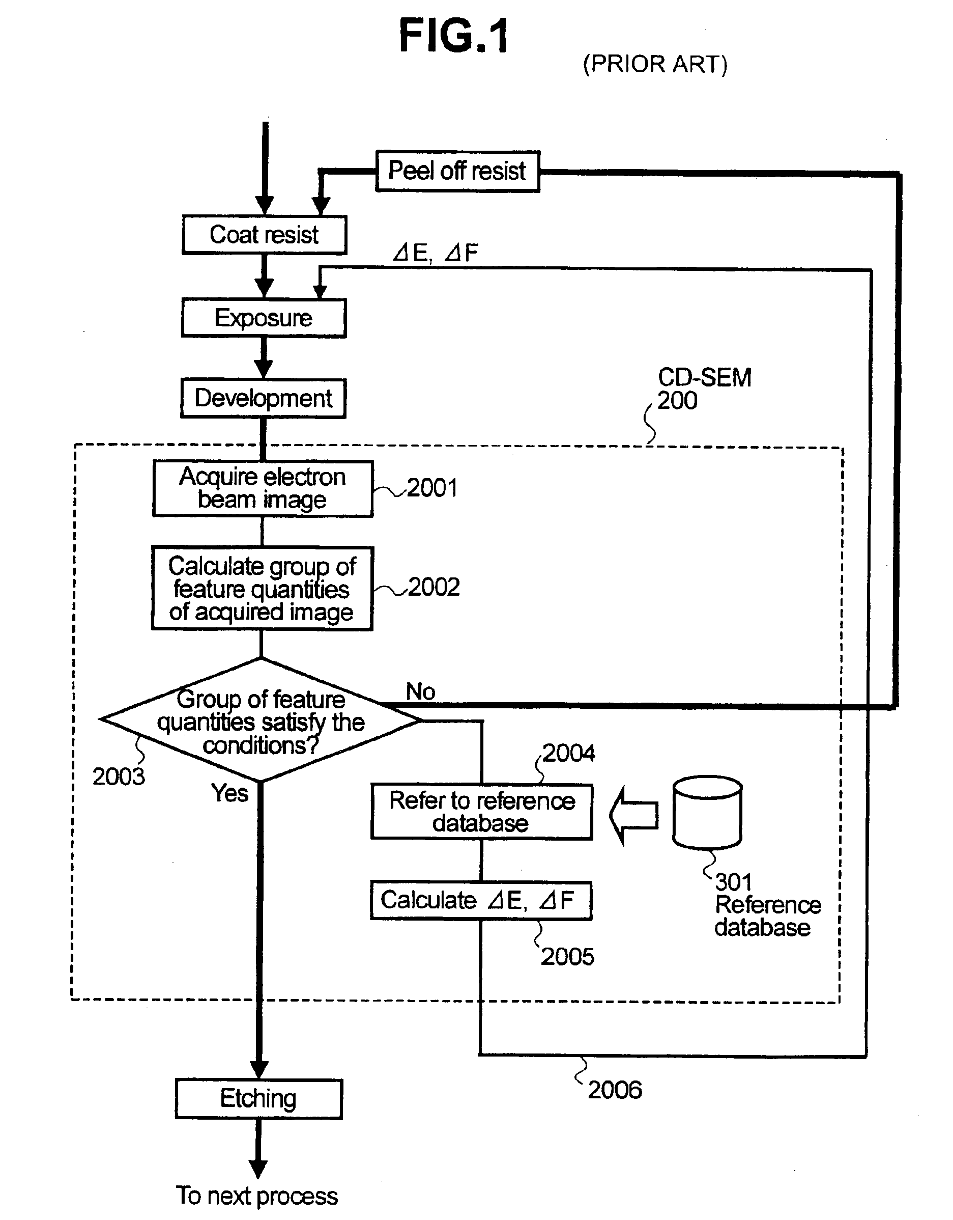
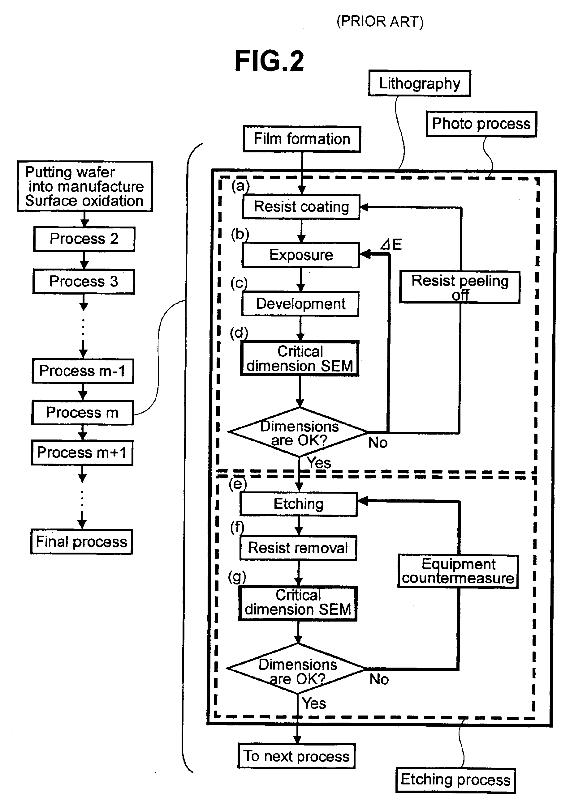
[0089]FIG. 1 is a conceptual diagram of the lithography process, according to the first embodiment of the present invention, that uses a lithography-process monitoring system constructed on a CD-SEM 200 (the outline composition is shown in FIG. 10). In this embodiment, the CD-SEM generates the electron beam image (step 2001), subsequently calculates a group of feature quantities (details will be described later) that represent characteristics of a 3-D shape of the resist pattern from the electron beam image (step 2002), evaluates the 3-D shape based on the group of feature quantities, and, at the same time, calculates feedback quantities ΔE and ΔF to the exposure condition parameters (the exposure and the focus) by using a reference database 301 (details will be described later) that has previously been constructed using the FEM wafer (step 2003-2005).

[0090]FIG. 42 shows an example of the composition of a semiconductor production line that incl...

second embodiment

[0130]FIG. 21(a) shows a processing sequence in the lithography process monitoring system constructed on the CD-SEM 200, according to a second embodiment of the present invention.

[0131]In FIG. 21(a), the steps 2001-2005, in which calculation of ΔE and ΔF is fully achieved, are the same as in the first embodiment. Subsequently, ΔE and ΔF, as they are, are not fed back to the exposure equipment, but the feedback quantities ΔE1 and ΔF1 are determined by referring to a history database 303 and using the information of past ΔE and ΔF. For example, in the history database 303, ΔE and ΔF for a few lots in the past are stored, and definitive feedback quantities ΔE1 and ΔF1 are determined by approximating the history data with a straight line, as shown in FIG. 21(b).

[0132]Even under the same exposure and the same focus, a completely identical resist pattern is not necessarily produced when observing it microscopically, and, in addition, ΔE and ΔF that were calculated from each subject of the...

third embodiment

[0134]FIG. 22(a) shows a processing sequence of the lithography-process monitoring system constructed on the CD-SEM 200, according to a third embodiment of the present invention.

[0135]In the first and second embodiments, it is only when the group of feature quantities do not satisfy the conditions at the step 2003 the routine of calculating ΔE and ΔF is performed. However, in this embodiment, even when the group of feature quantities of the subject of the inspection satisfy the conditions, referring to the history database 303 and based on the trends of variations of ΔE and ΔF from the past, the situations in the future are predicted; and, if necessary, fine tuning of the exposure conditions (Δe, Δf) is executed.

[0136]In FIG. 22(b), a range between the alternate long and short dash lines represents a process window. The exposure tends to be on an upward trend and in the next run the exposure is at a risk of going out of the process window. On the other hand, the focus tends to be on...


PUM


Abstract

To realize a method for detecting variations in conditions (drift of the exposure and drift of the focus) in exposure equipment at a product wafer level in lithography process, the process is specified in such a way that calculation results of feature quantities such as electron beam images, line profiles, dimensions, etc. under various sets of the exposure and the focus are stored as a library, and an electron beam image of the product wafer is compared with these pieces of data in the library so that detection of drifts of the exposure and the focus a check of the results on the screen can easily be performed.

Description

BACKGROUND OF THE INVENTION[0001]The present invention relates to a method of monitoring processes used in the manufacture of semiconductor devices, such as a lithography process and an etching process, and a system therefore; and, more specifically, the invention relates to a method of monitoring the manufacture of a semiconductor device so as to monitor a state of processing in each process from an image obtained by imaging a pattern produced on a substrate that was processed in each treatment process, and a system therefor.[0002]FIG. 2 is a view showing the flow of processing in a conventional lithography process. The lithography process consists of a photo process in which a resist pattern is formed by exposure and development, and an etching process in which the resist pattern is transferred onto a film that is the subject of the processing.[0003]A thin film of a material to be processed is first grown on a substrate of a semiconductor wafer. Then, a resist pattern is produced ...

Claims


Application Information

Patent Timeline
IPC IPC(8): H01L21/00
CPCH01L21/67276
Inventor SHISHIDO, CHIETAKAGI, YUJIWATANABE, MASAHIROYOSHITAKE, YASUHIROMATSUMOTO, SHUNICHIIIZUMI, TAKASHIKOMURO, OSAMUTANAKA, MAKIMOROKUMA, HIDETOSHI
Owner HITACHI LTD
Why Eureka
Try Eureka