
System and method for chip testing

Inactive Publication Date: 2005-06-21
HEWLETT-PACKARD ENTERPRISE DEV LP +1
View PDF8 Cites 23 Cited by
  • Summary
  • Abstract
  • Description
  • Claims
  • Application Information

AI Technical Summary

Benefits of technology

[0015]The system and method of the present invention are particularly advantageous over the prior art because an innovative and universal BIST circuit is designed to be completely configurable and to transmit detailed failure information off-chip, under command of a simple and inexpensive personal computer (PC). Thus the present invention replaces very expensive and difficult to use logic testing devices, and is particularly useful when testing system on a chip designs.

Problems solved by technology

However, chip testing has become much more complex with the advent and popularity of modem System On a Chip (SOC) designs.
Since memory testers are not capable of testing logical circuitry, manufactures have been forces to use logic testers for testing the SOCs.
Unfortunately, since logic testers were never intended to test chips with large memory arrays, test routines within the logic testers have become awkwardly complex as test engineers have tried to program them to test such memory arrays.
While BIST circuits enable the chip to perform testing on itself, the silicon resources necessary to build these BIST circuits on the chip adds significant complexity to the chip and taking away silicon resources that could otherwise have been reallocated.
Furthermore, most BIST circuits only generate and transmit out a pass / fail signal which by itself provides no detailed information which could enable these manufacturers to repair the chip, by such techniques as redundancy allocation, without again performing a conventional logic and / or memory array test with a logic tester as described above.
The ROM contains a fixed micro-code, however, has several limitations.
First the micro-code can not be modified once burned in ROM.
Second, the micro-code executed test routines are rigid and un-modifiable.
Third, the ROM and BIST circuitry together are almost equivalent to a second CPU / SOC design in themselves, which requires a significant customized design effort in itself, as well as significant silicon resources.
Also, since memory defects are very much foundry sensitive, none of the above described BIST algorithms can be universally applied to a large number of logic and / or memory chips, which each currently require unique, customized, and rigid conventional memory testing.
Standardized BIST ROMs or circuits simply can not be designed to affect all the different test algorithms which each separate foundry requires.
Thus, well known and laborious “direct memory testing” techniques, which use a large numbers of pads and associated complex pad multiplexing functions, have largely remained as the only way to perform embedded memory testing, especially for embedded DRAM.
Such testing is however, very costly in terms of testing time and capital equipment expense.

Method used


Image

  • System and method for chip testing
  • System and method for chip testing
  • System and method for chip testing

Examples


Embodiment Construction

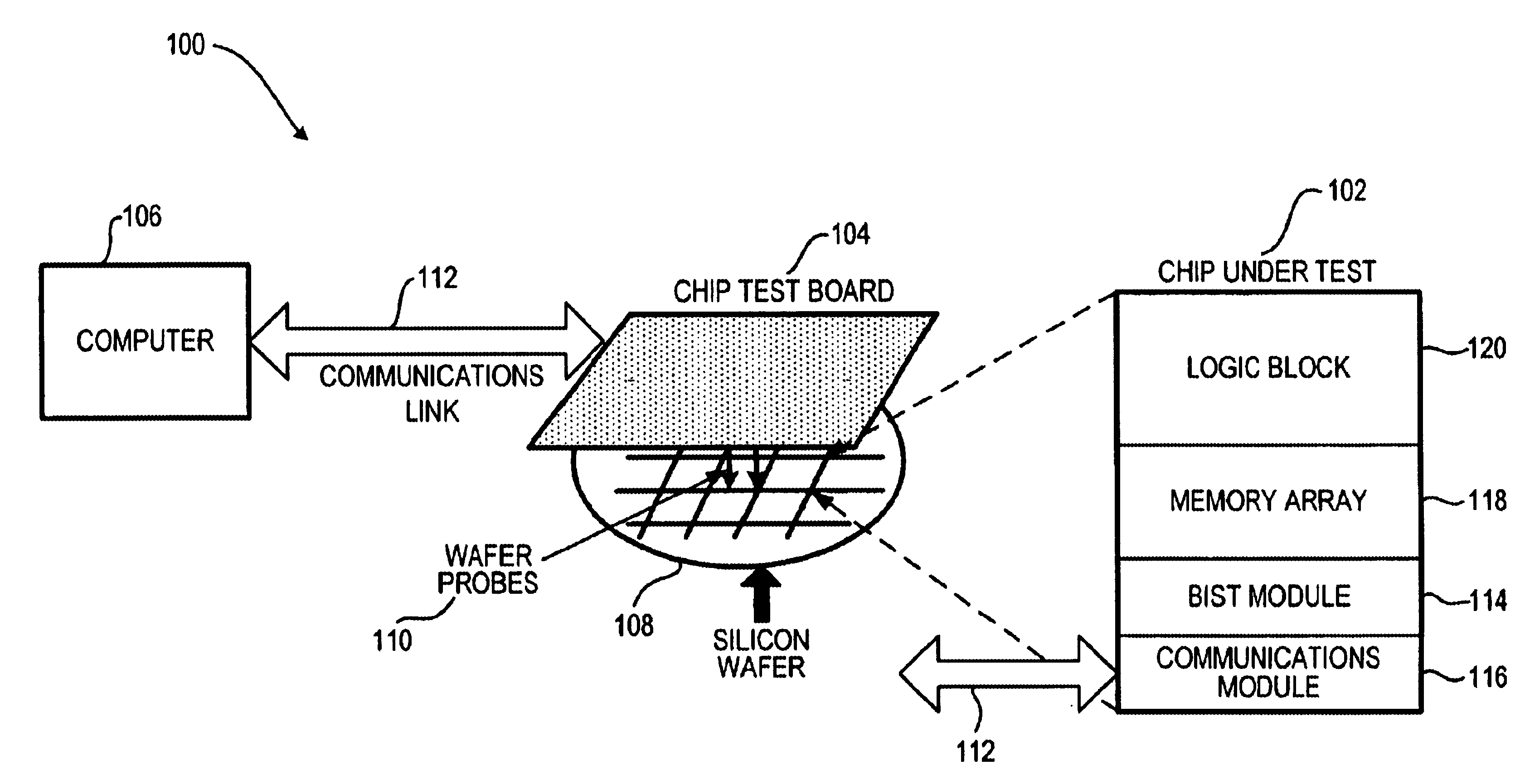
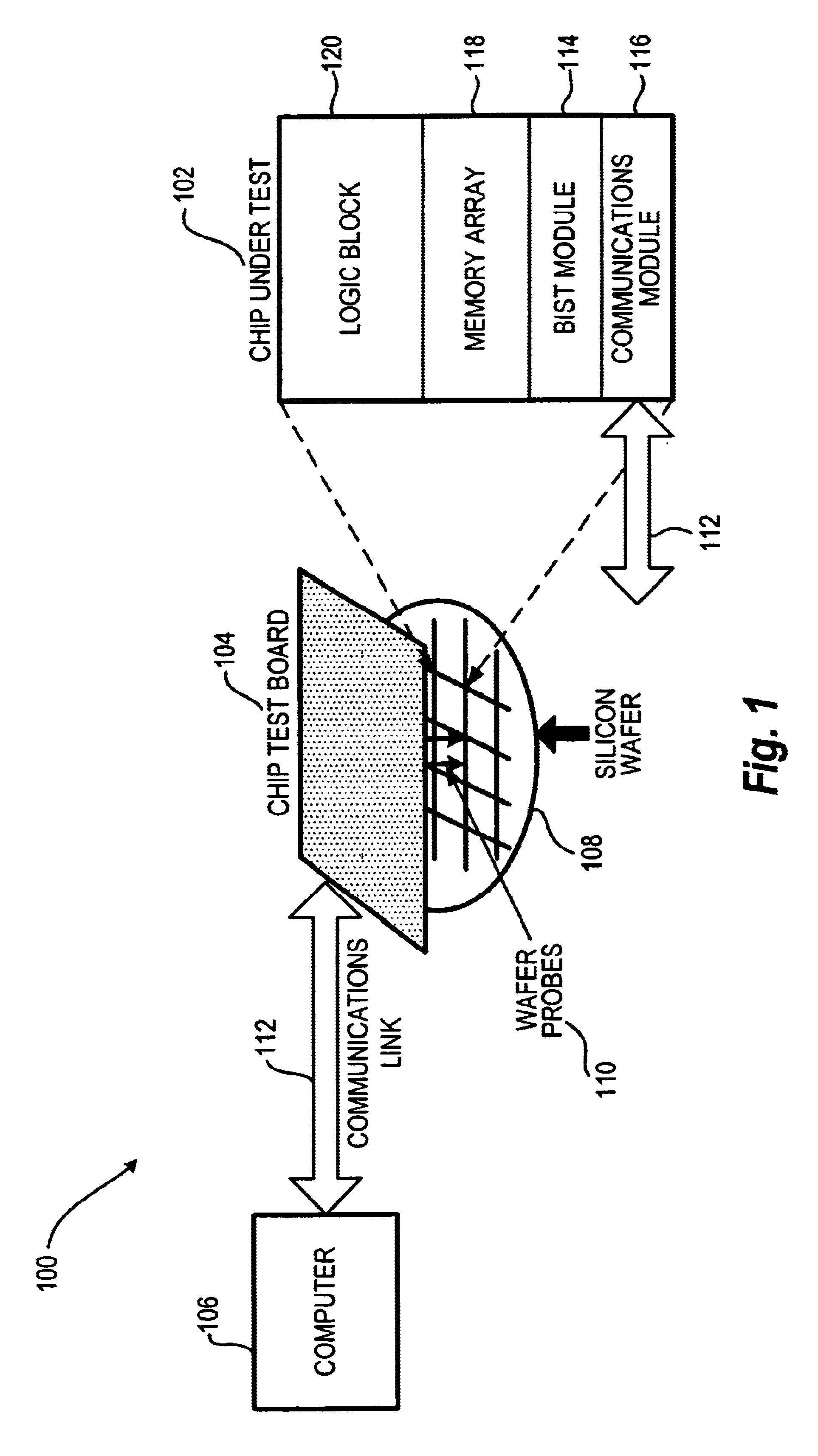
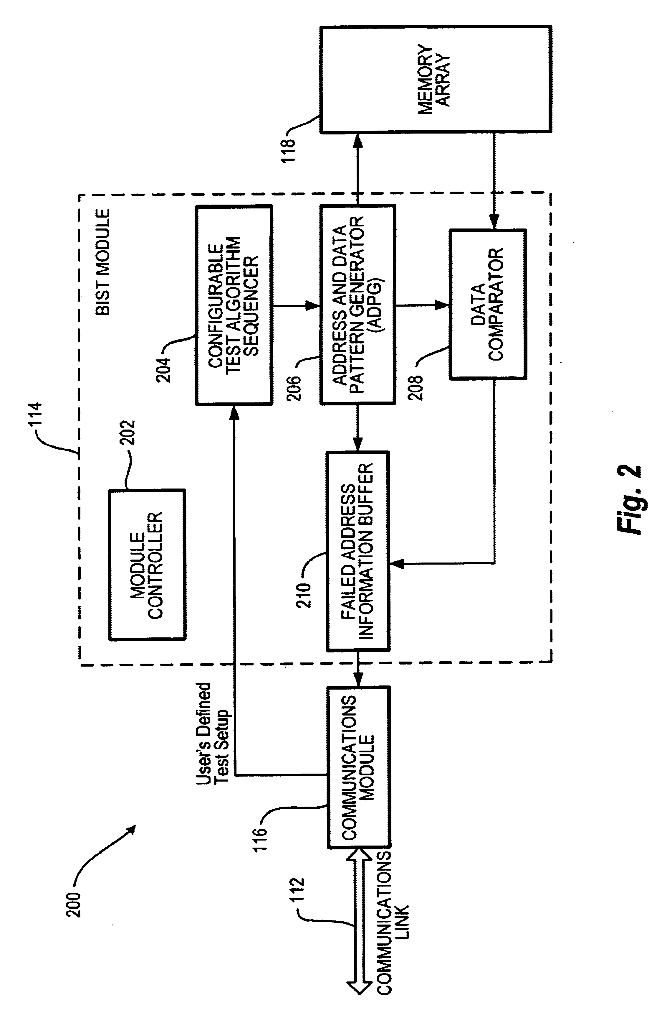
[0021]FIG. 1 is a block diagram of an embodiment of a system 100 for testing an embedded memory array. The system 100 includes a chip under test 102, a chip test board 104 and a computer tester 106. The chip 102 is an integrated circuit preferably tested while still a part of an intact silicon wafer 108 and is in communication with the test board 104 through conventional wafer probes 110. The computer 106 is preferably a conventional computer operating a set of chip testing software, but in an alternative embodiment, can be replaced by a logic tester. The chip 102 and computer 106 exchange messages via a communications link 112. The communication link 112 is preferably passes the messages according to one of several conventional serial bus protocols, such as JTAG (IEEE 1149.1), RS-232, 12C, SMBus, Universal Serial Bus (USB) 1.1 or 2.0, Firewire (IEEE 1394), or others. The message is preferably sent serially so as to minimize chip complexity and thus minimize chip costs. Those skille...


PUM


Abstract

A system and method for chip testing is disclosed. The present invention's method includes the steps of establishing a communications link between a chip and a computer tester; receiving on the chip an initial test algorithm over a communications link; testing the chip, using a built-in self-test (BIST) circuit on the chip, in accordance with the initial algorithm; collecting a set of failure information in response to testing; and transmitting the failure information from the chip to the computer over the communications link. The present invention's system includes: a communications link; a computer, operating a set of chip testing software; and a chip under test coupled to the computer by the communications link, having, a memory array; and a BIST module for testing the memory array in response to test algorithms received from the computer and transmitting those addresses within the memory array which failed testing.

Description

BACKGROUND OF THE INVENTION[0001]1. Field of the Invention[0002]The present invention relates generally to systems and methods for testing silicon wafers, and more particularly for chip testing.[0003]2. Discussion of Background Art[0004]Currently there are two major types of silicon chip testers: logic testers and memory testers. Both types of testers include very specialized routines for performing high throughput chip testing. However, chip testing has become much more complex with the advent and popularity of modem System On a Chip (SOC) designs. SOC designs incorporate both logic and memory circuitry. Since memory testers are not capable of testing logical circuitry, manufactures have been forces to use logic testers for testing the SOCs. Unfortunately, since logic testers were never intended to test chips with large memory arrays, test routines within the logic testers have become awkwardly complex as test engineers have tried to program them to test such memory arrays. Such ba...

Claims


Application Information

Patent Timeline
IPC IPC(8): G01R31/3193G01R31/28G01R31/3187G01R31/319G11C29/48G11C29/04
CPCG01R31/3187G01R31/31926G01R31/31935G11C29/48G11C11/41G11C2029/5604G11C2029/5606
Inventor KU, JOSEPH WEIYEH
Owner HEWLETT-PACKARD ENTERPRISE DEV LP
Learn More