Conductive bi-layer e-beam resist with amorphous carbon

a technology of amorphous carbon and conductive bi-layers, applied in the field of integrated circuit (ic) fabrication methods, can solve the problems of reducing the resolution of the pattern, ics have evolved into complex devices, and conventional photolithographic techniques have a lower limit in the dimension of the pattern that may be formed

Inactive Publication Date: 2005-07-05
APPLIED MATERIALS INC
View PDF4 Cites 14 Cited by
  • Summary
  • Abstract
  • Description
  • Claims
  • Application Information

AI Technical Summary

Problems solved by technology

In recent years ICs have evolved into complex devices that commonly include millions of transistors, capacitors, resistors, and other electronic components on a single chip.
Due to limitations in mask formation and associated diffraction effects, however, conventional photolithographic techniques have a lower limit in the dimension of pattern that may be formed.
However, depending on properties of resist material, at higher accelerating voltages, forward scattering of electrons may occur as the electrons travel through the resist material, which may reduce pattern resolution.
Further, backward scattering of the electrons may occur as the electrons reflect off a substrate or other material underlayer, and travel back through the e-beam resist which may also reduce pattern resolution.
The low penetration depth of electrons associated with low voltage e-beam pattern imaging typically necessitates a relatively thin e-beam resist layer which, alone, may have an insufficient etch resistance for use as a mask layer in subsequent pattern transfer etching processes.
However, one problem with a non-conductive mask layer 104 is a possible accumulation of electrons at or near a junction of the mask layer 104 and the e-beam resist layer 106.

Method used


Image

  • Conductive bi-layer e-beam resist with amorphous carbon
  • Conductive bi-layer e-beam resist with amorphous carbon
  • Conductive bi-layer e-beam resist with amorphous carbon

Examples


Embodiment Construction

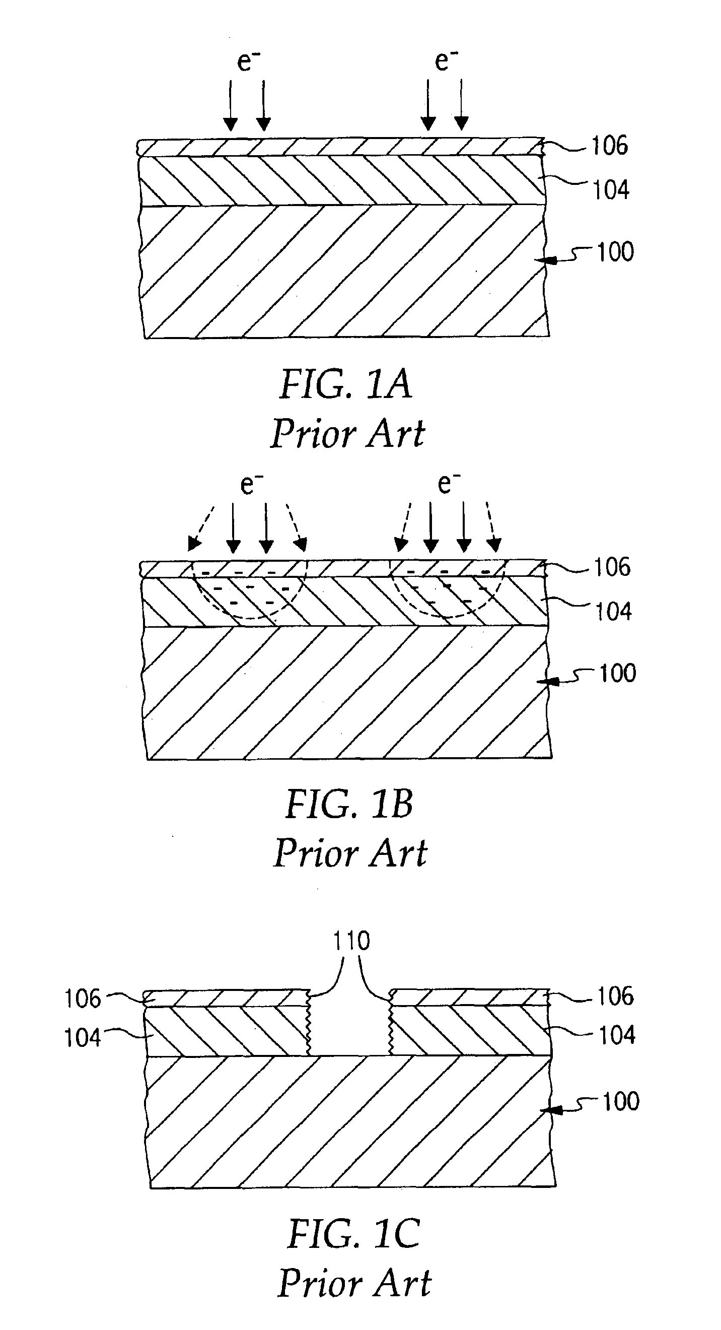
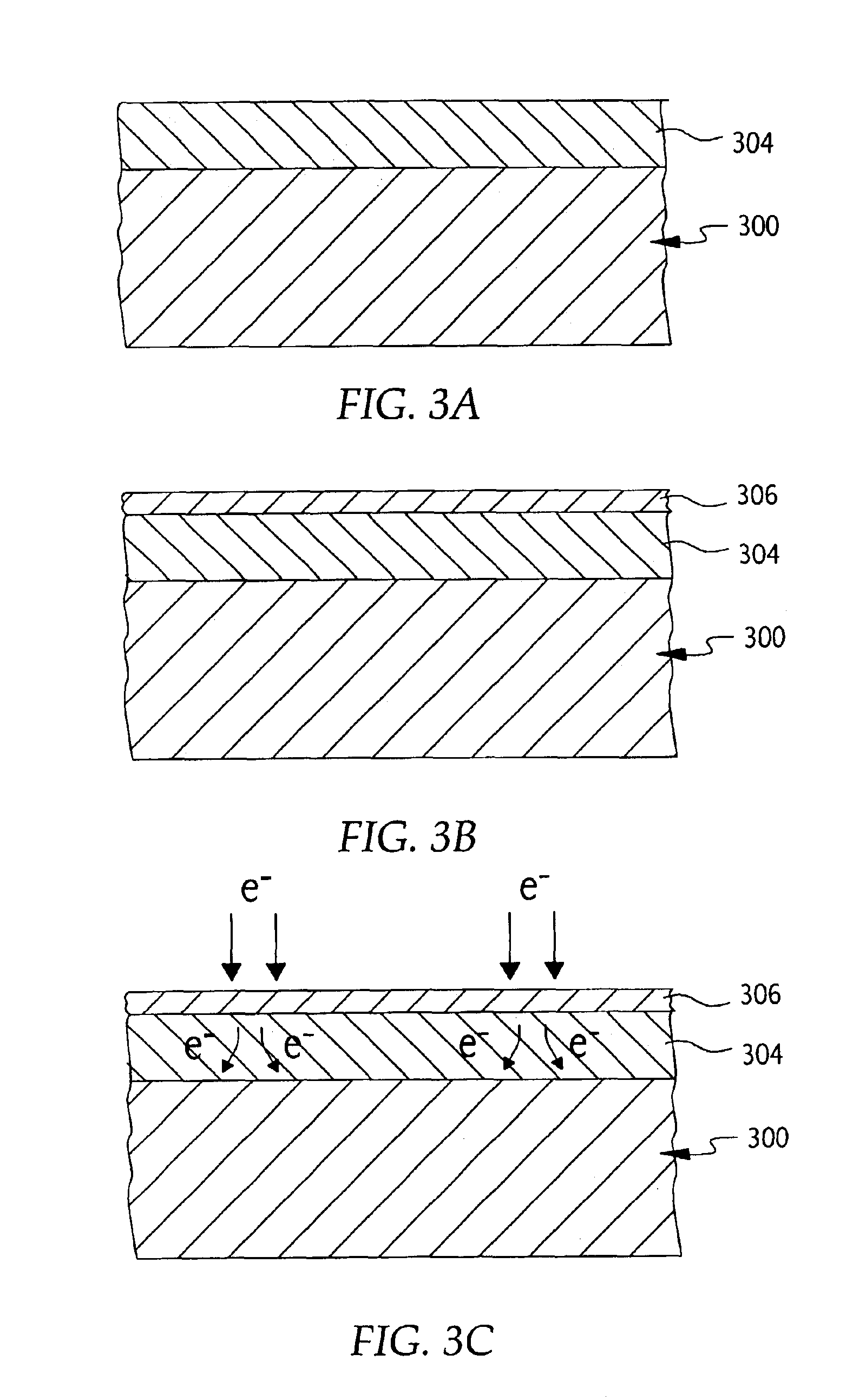
[0021]Embodiments of the present invention generally provide methods for forming integrated circuits utilizing a bi-layer resist formed by depositing a layer of electron beam (e-beam) sensitive resist material over a layer of amorphous carbon. A pattern may be formed in the e-beam resist layer via an e-beam writing process. During the e-beam writing process, electrons passing through the e-beam resist layer may be conducted away through the amorphous carbon layer, thereby preventing the buildup of electrons which may repel electrons from the e-beam resulting in a less focused e-beam and lower resolution pattern. As used herein, the term amorphous carbon generally refers to a carbon material without long-range crystalline order, and includes diamond like carbon (DLC) materials.

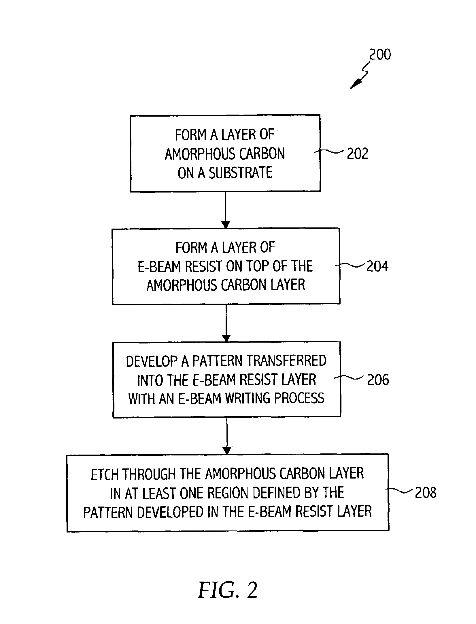
[0022]FIG. 2 illustrates exemplary operations 200 for forming a patterned amorphous carbon layer according to one embodiment of the present invention. The operations 200 may be described with reference to FIGS....


PUM

PropertyMeasurementUnit
accelerating voltageaaaaaaaaaa

Abstract

Methods for forming a patterned layer of amorphous carbon on a substrate are described. A layer of amorphous carbon may be formed on the substrate. A layer of electron sensitive resist may be formed on top of the amorphous carbon layer. A pattern transferred into the electron sensitive resist layer with an electron beam writing process is developed. During the electron beam writing process, electrons may be conducted away from the writing area through the amorphous carbon layer. The amorphous carbon layer may be etched through in at least one region defined by the pattern developed into the layer of electron sensitive resist material. For some embodiments, the amorphous carbon layer may be formed by chemical vapor deposition. For some embodiments, the layer of electron sensitive resist may be hydrogen silsesquioxane (HSQ).

Description

BACKGROUND OF THE INVENTION[0001]1. Field of the Invention[0002]Embodiments of the present invention generally relate to integrated circuit (IC) fabrication methods, and more particularly, to electron beam lithography methods for use in forming patterns in material layers of an IC.[0003]2. Description of the Related Art[0004]In recent years ICs have evolved into complex devices that commonly include millions of transistors, capacitors, resistors, and other electronic components on a single chip. Therefore, there is an inherent demand for increased circuit densities, as well as a continual demand for faster and more efficient circuit components. The combined demands for faster circuits having greater circuit densities imposes corresponding demands on the materials used to fabricate such integrated circuits, as well as on process sequences used for IC fabrication.[0005]For example, in process sequences using conventional photolithographic techniques, a layer of photo-sensitive resist ...

Claims


Application Information

Patent Timeline
Patent Type & Authority Patents(United States)
IPC IPC(8): G03C5/00G03F1/00G03F1/68G03F7/09G03F7/20
CPCG03F1/68G03F7/093G03F7/2059G03F1/0015H01J2237/31754Y10S430/143
Inventor BENCHER, CHRISTOPHER D.LATCHFORD, IAN S.
Owner APPLIED MATERIALS INC
Why Eureka
Try Eureka