Structure and manufacturing method for GaN light emitting diodes

a manufacturing method and light-emitting diode technology, applied in the direction of basic electric elements, electrical apparatus, semiconductor devices, etc., can solve the problems of difficult to improve the operating voltage (vf), and the structure and its ohmic contact of the conventional gan led manufactured with the aforementioned method have a drawback, so as to achieve superior photo-penetration and reduce resistance

Inactive Publication Date: 2005-07-05
FORMOSA EPITAXY INCORPORATION +1
View PDF7 Cites 38 Cited by
  • Summary
  • Abstract
  • Description
  • Claims
  • Application Information

AI Technical Summary

Benefits of technology

[0008]The present invention employs a material of indium tin oxide, which has a superior photo-penetrability, to replace the Ni/Au in forming the transparent conductive layer 7. However, because of the lack of an ohmic contact between the ITO mate

Problems solved by technology

However, the structure and its ohmic contact of the conventional GaN LED manufactured with the aforementioned method have a drawb

Method used


Image

  • Structure and manufacturing method for GaN light emitting diodes
  • Structure and manufacturing method for GaN light emitting diodes
  • Structure and manufacturing method for GaN light emitting diodes

Examples


Embodiment Construction

[0019]The preferred embodiment of the present invention is described as below. However, some parts of the figures are not drawn in accordance with the physical proportion due to the illustrative purpose. The emphasis on some parts or components is to provide a more clear description of the invention to those who are skilled in this field.

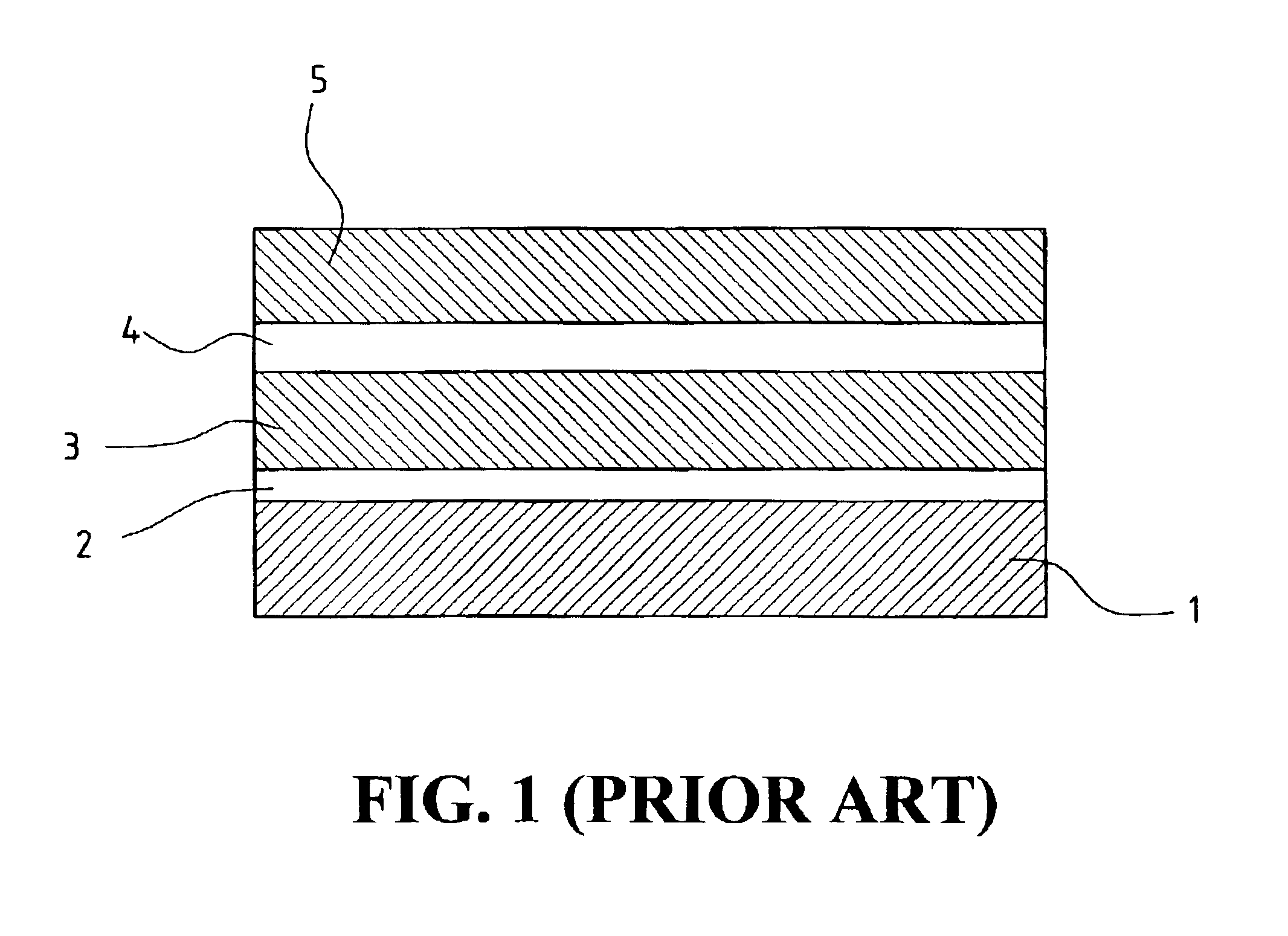
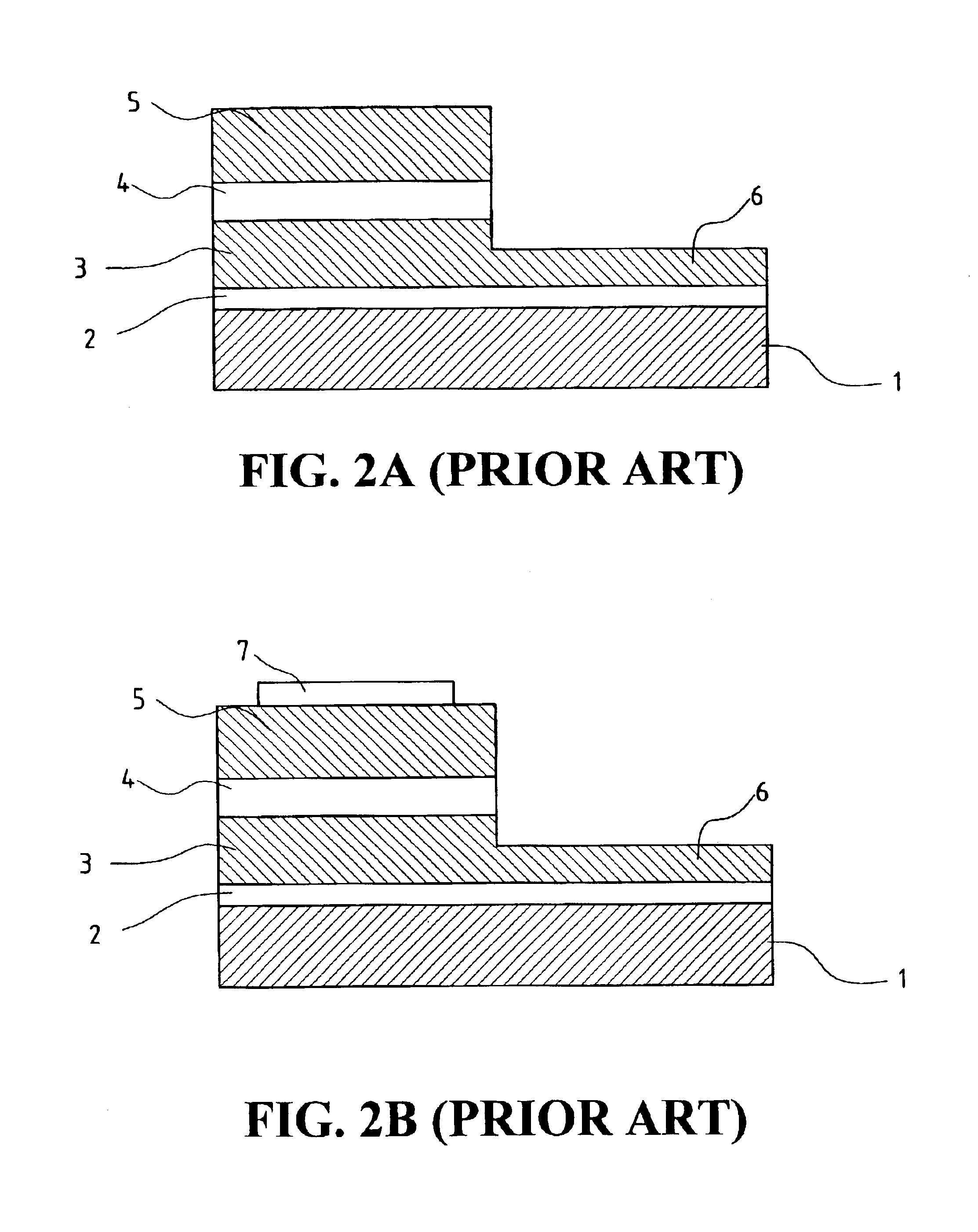
[0020]As shown in FIG. 3, a substrate 10 is provided. A buffer layer 20 is formed on the substrate 10 by using metal organic chemical vapor deposition (MOCVD), molecular beam epitaxy, vapor phase epitaxy (VPE), or liquid phase epitaxy (LPE). The present invention prefers the MOCVD method. By using the same method, an N-type GaN layer 30 is formed on top of the buffer layer 20, a light-emitting stack layer 40 is formed on top of the N-type GaN layer 30, a P-type GaN layer 50 is formed on top of the light-emitting stack layer 40, and finally, a digital transparent layer 100 is formed on top of the P-type GaN layer 50. The cross section of the digital ...


PUM


Abstract

A GaN semiconductor stack layer is formed on top of a substrate for manufacturing a light emitting diode. The GaN semiconductor stack layer includes, from the bottom up, an N-type GaN contact layer, a light emitting stack layer and a P-type contact layer. The next step is to form a digital transparent layer on the P-type GaN contact layer, then use dry etching technique to etch downward through the digital transparent layer, the P-type GaN contact layer, the light emitting layer, the N-type GaN contact layer, and form an N-metal forming area within the N-type GaN contact layer. The next step is to form a first ohmic contact electrode on the P-type contact layer to serve as P-type ohmic contact, and a second ohmic contact electrode on the N-metal forming area to serve as N-type ohmic contact. Finally, a bump pad is formed on the first ohmic contact electrode and the second ohmic contact electrode, respectively.

Description

FIELD OF THE INVENTION[0001]This invention relates to a structure and a manufacturing method for light emitting diodes (LED), and more specially to a structure and a manufacturing method for ohmic contact of light emitting diodes made of GaN or other wide bandgap materials.BACKGROUND OF THE INVENTION[0002]As shown in FIG. 1, a conventional GaN light emitting diode has a structure comprising a substrate 1, a buffer layer 2 formed on top of the substrate 1, an N-type GaN layer 3 formed on top of the buffer layer 2, a light emitting stack layer formed on top of the N-type GaN layer 3, and a P-type GaN layer 5 formed on top of the light emitting stack layer 4. As shown in FIG. 2A, using the inductively coupled plasma-reactive ion etching (ICP-RIE) dry etching technique, the structure of FIG. 1 is etched downwards through the P-type GaN layer 5, light emitting stack layer 4, and a portion of the N-type GaN layer 3 to form an N-Metal forming area 6 of depth about 10,000Å. As shown in FIG....

Claims


Application Information

Patent Timeline
IPC IPC(8): H01L33/00H01L33/04H01L33/14H01L33/32H01L33/42
CPCH01L33/14H01L33/32H01L33/04H01L33/42
Inventor CHEN, LUNG-CHIENLAN, WEN-HOWCHIEN, FEN-REN
Owner FORMOSA EPITAXY INCORPORATION
Why Eureka
Try Eureka