Method of forming bumps

a technology of bumps and bumps, applied in the direction of semiconductor devices, semiconductor/solid-state device details, electrical equipment, etc., can solve the problems exposing the back of flip-chip dies to increase heat dissipation, etc., and achieve the effect of reducing the size variation between solder blocks

Inactive Publication Date: 2005-07-12
ADVANCED SEMICON ENG INC
View PDF5 Cites 12 Cited by
  • Summary
  • Abstract
  • Description
  • Claims
  • Application Information

AI Technical Summary

Benefits of technology

[0012]Accordingly, one object of the present invention is to provide a method of forming bumps capable of reducing size variation between solder blocks.
[0013]A second object of this invention is to provide a method of forming bumps capable of reducing the production of voids inside solder blocks.
[0014]A third object of this invention is to provide a method of forming bumps capable of reducing distance of separation between neighboring solder blocks so that a higher packing density is possible.
[0015]A fourth object of this invention is to provide a method of forming bumps capable of reducing the occurrence of missing block condition.
[0018]Since the solder blocks are prefabricated before being disposed into the openings in the photoresist layer, shape and interior constituents of the solder block can be carefully controlled. With careful control of the fabrication process, number and size of voids inside each solder block can be set within an acceptable range. Thus, reliability of the bond between the solder block and the substrate as well as between the solder block and the under-ball metallic layer is improved. Because the size of each solder block is uniform, the solder block is at a standard height level above the under-ball metallic layer after a reflow process. Moreover, the size of the openings in the photoresist layer can be greatly reduced. Only if the solder blocks with a standard size can be accommodated into the openings, the openings formed can be as small as possible. With smaller openings, the distance between neighboring solder blocks can be reduced and a higher-density package can be produced. In addition, if a solder block is missing or does not fit into a particular opening, the vacant or misfit location can be easily found by visual inspection. Ultimately, missing block conditions will rarely occur.

Problems solved by technology

Moreover, the back of a flip-chip die may be exposed to increase heat dissipation.
Hence, the solder blocks 150 must be separated from each other by a considerable distance, rendering the production of higher-density packages difficult.

Method used


Image

  • Method of forming bumps
  • Method of forming bumps
  • Method of forming bumps

Examples


Embodiment Construction

[0025]Reference will now be made in detail to the present preferred embodiments of the invention, examples of which are illustrated in the accompanying drawings. Wherever possible, the same reference numbers are used in the drawings and the description to refer to the same or like parts.

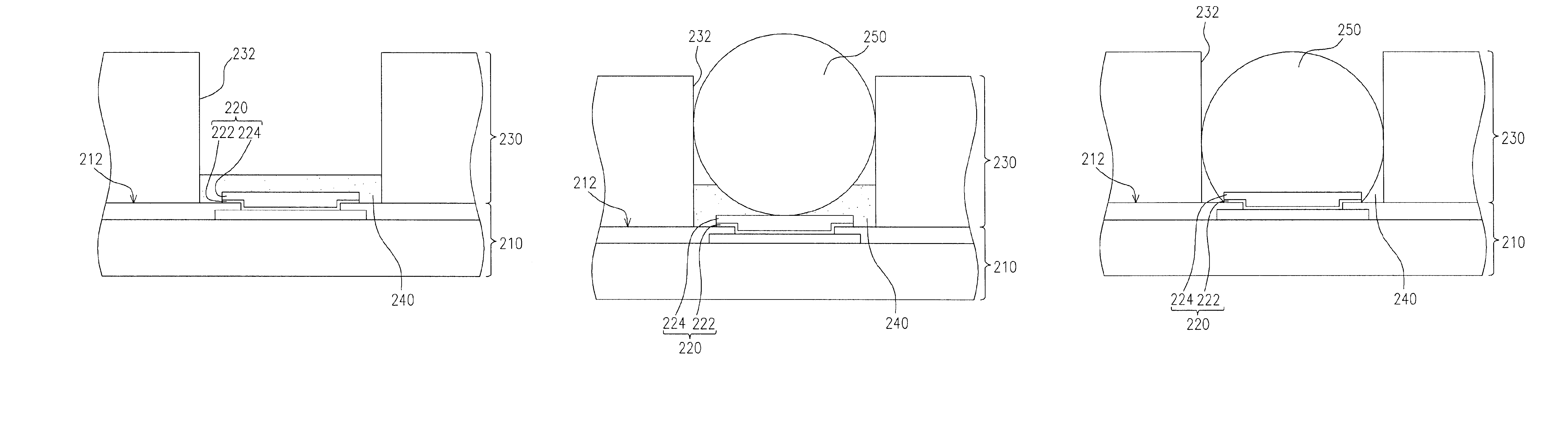
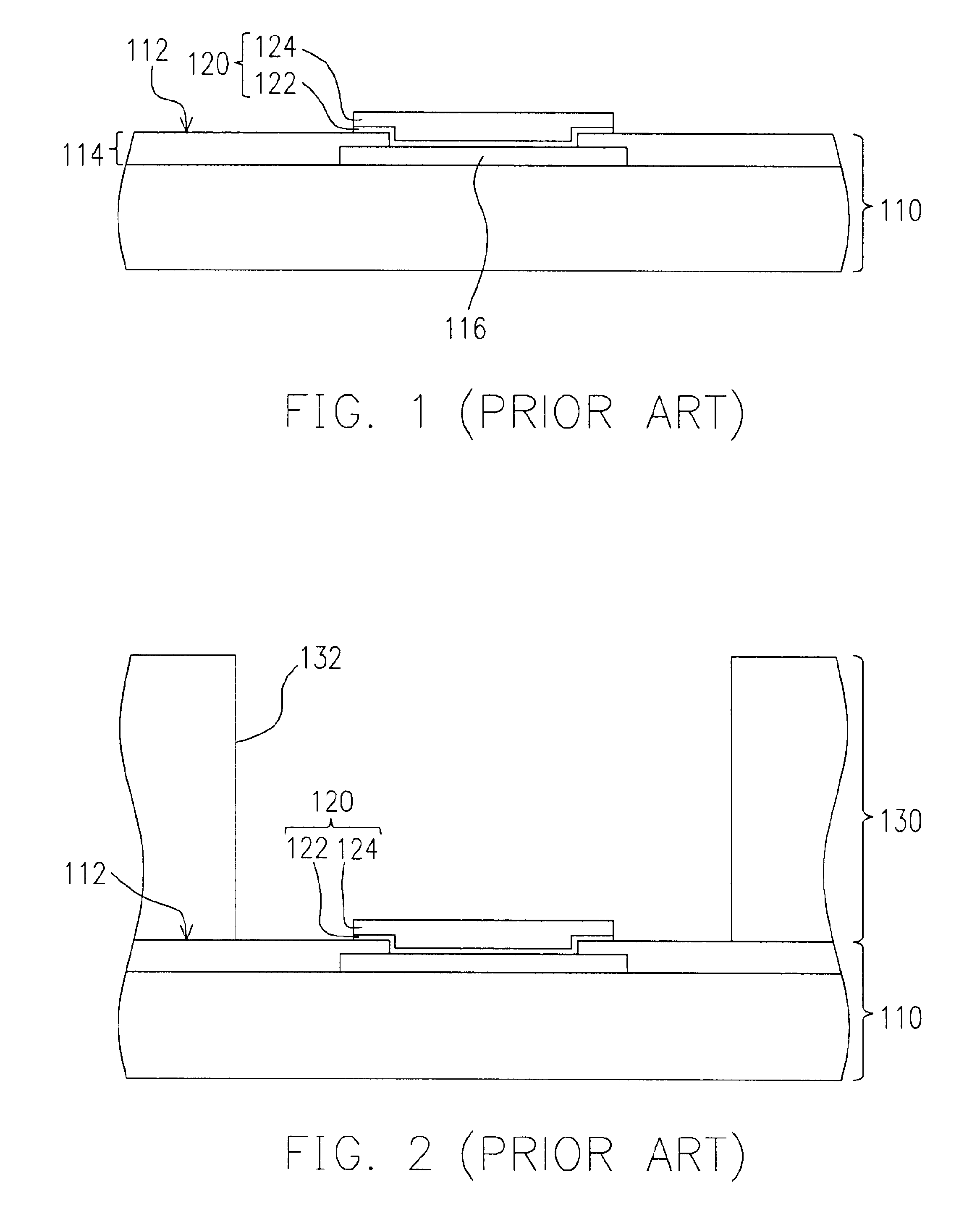
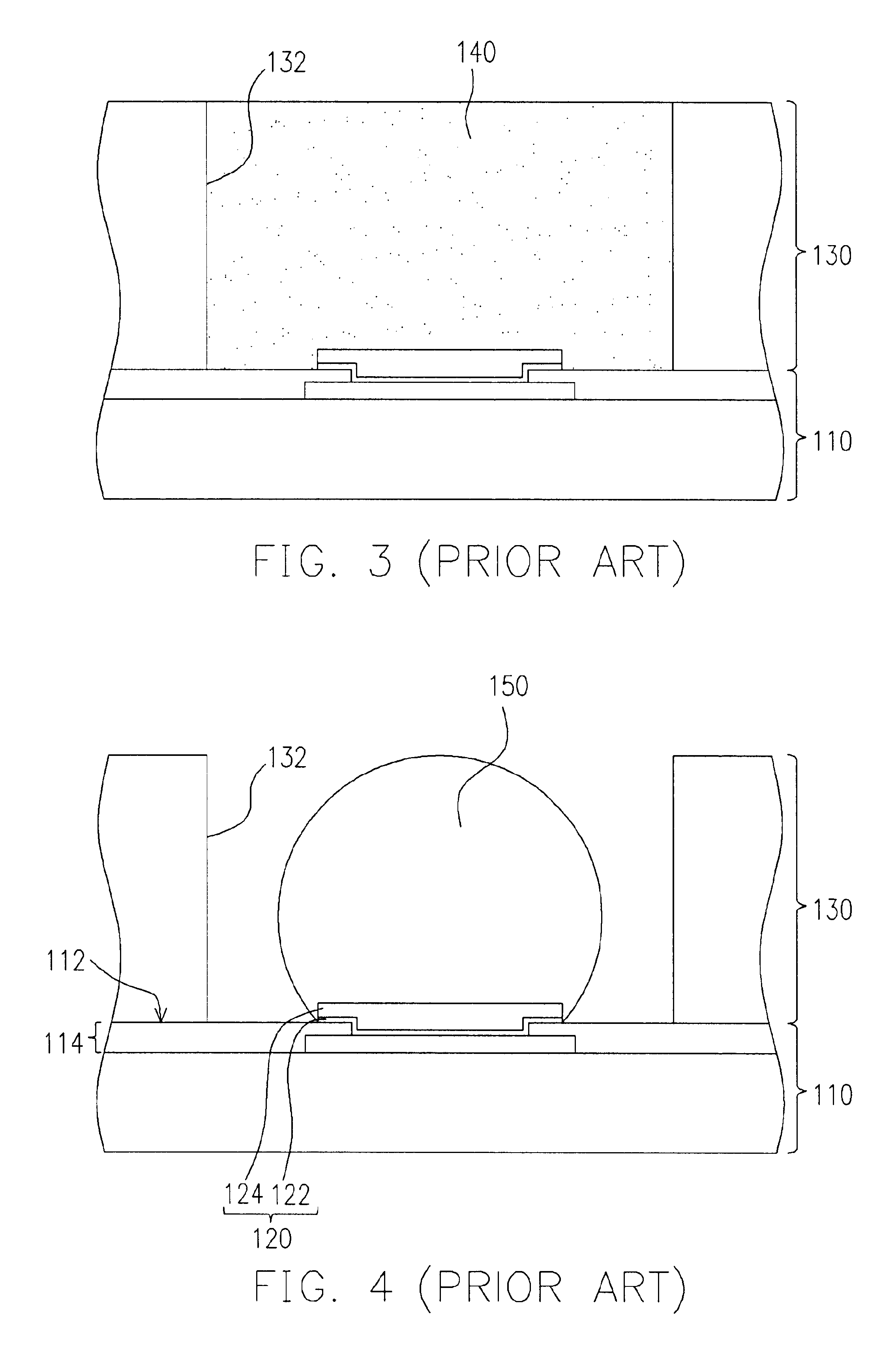
[0026]FIGS. 6 through 11 are partially magnified cross-sectional views showing the progression of steps for forming a bump on the surface of a chip according to one preferred embodiment of this invention. As shown in FIG. 6, a silicon wafer 210 having an active surface 212 thereon is provided. The active surface 212 of the wafer 210 further includes a passivation layer 214 and a plurality of contact pads 216 (only one is shown). The passivation layer 214 exposes the contact pads 216. The contact pads 216 are aluminum or copper pads, for example. A process for forming an under-ball metallic layer 220 over the contact pad 216 is conducted. First, an adhesion layer 222 is formed over the active layer 21...


PUM


Abstract

A method of forming a plurality of bumps over a wafer. The wafer has an active surface having a passivation layer and a plurality of contact pads thereon. The passivation layer exposes the contact pads on the active surface. An adhesion layer is formed over the active surface of the wafer and covers both the contact pads and the passivation layer. A metallic layer is formed over the adhesion layer. The adhesion layer and the metallic layer are patterned so that the adhesion layer and the metallic layer remain on top of the contact pads. A photoresist layer is formed on the active surface of the wafer. The photoresist layer has a plurality of openings that expose the metallic layer. Flux material is deposited into the openings and then a solder block is disposed into each of the openings. A reflow process is carried out so that the solder block bonds with the metallic layer. Finally, the flux material and the photoresist layer are removed.

Description

CROSS REFERENCE TO RELATED APPLICATIONS[0001]This application claims the priority benefit of Taiwan application Ser. No. 91115993, filed Jul. 18, 2003.BACKGROUND OF INVENTION[0002]1. Field of Invention[0003]The present invention relates to a method of forming bumps. More particularly, the present invention relates to a method of forming high-quality bumps inside a high-density package.[0004]2. Description of Related Art[0005]In this information explosion age, integrated circuit products are used almost everywhere in our daily life. As fabricating technique continue to improve, electronic products having powerful functions, personalized performance and a higher degree of complexity are produced. Nowadays, most electronic products are relatively light and have a compact body. Hence, in semiconductor production, various types of high-density semiconductor packages have been developed. Flip chip is one of the most commonly used techniques for forming an integrated circuit package. In a ...

Claims


Application Information

Patent Timeline
Patent Type & Authority Patents(United States)
IPC IPC(8): H01L21/4763H01L23/488H01L21/02H01L21/44H01L23/48H01L21/60H01L27/15H01L29/267H01L31/12H01L33/00
CPCH01L24/11H01L2224/1147H01L2224/13099H01L2224/16H01L2924/01012H01L2924/01013H01L2924/01022H01L2924/01029H01L2924/0103H01L2924/01046H01L2924/01047H01L2924/01049H01L2924/01051H01L2924/01073H01L2924/01074H01L2924/01078H01L2924/01079H01L2924/01082H01L2924/04941H01L2924/04953H01L2924/14H01L2924/01023H01L2924/01024H01L2924/01033H01L2924/014H01L2224/11334H01L24/03H01L24/05H01L24/13H01L2224/023H01L2224/03828H01L2224/05001H01L2224/05022H01L2224/05027H01L2224/0508H01L2224/05172H01L2224/05572H01L2224/11849H01L2224/05644H01L2924/00014H01L2224/05647H01L2224/05655H01L2224/05664H01L2224/05666H01L2224/05671H01L2224/05681H01L2224/05124H01L2224/05147H01L2224/05166H01L2224/05171H01L2224/05184H01L2924/0001
Inventor WU, TSUNG-HUAHUANG, MIN-LUNGLEE, SHIH-CHANGFANG, JEN-KUANGYEH, YUNG-I
Owner ADVANCED SEMICON ENG INC
Why Eureka
Try Eureka