Systems and methods for multi-dimensional inspection and/or metrology of a specimen

a three-dimensional inspection and specimen technology, applied in the direction of optically investigating flaws/contamination, measurement devices, instruments, etc., can solve the problems of excessive current draw through the probe card, tester downtime, and incur tester repair costs

Inactive Publication Date: 2005-07-12
KLA TENCOR TECH CORP
View PDF27 Cites 64 Cited by
  • Summary
  • Abstract
  • Description
  • Claims
  • Application Information

AI Technical Summary

Benefits of technology

[0016]Systems and methods capable of performing high speed inspection and metrology of a specimen such as a bumped wafer are provided. An embodiment relates to a system configured to assess a dimension of a feature on a specim...

Problems solved by technology

Bumps that are incorrectly formed on a wafer may cause significant problems during further processing such as probing of the wafer and during use of the device.
For example, incorrectly formed bumps may damage probes on a probe card thereby causing tester downtime and incurring tester repair costs.
Incorrectly formed bumps may also bridge power and ground contacts thereby resulting in excessive current draw through a probe card.
In addition, incorrectly formed bumps may not be detected during probing and may increase the potential for failure of a packaged device.
Furthermore, probing may damage bumps especially on a wafer having a relatively high number of bumps per unit area that may require high vertical forces during testing to seat probes for proper contact.
Because currently available methods are generally not capable of simultaneous 2D and 3D data acquisition, such methods may be significantly slower than either 2D or 3D data acquisition.
In addition, 3D data acquisition may be significantly slower than 2D data acquisition thereby resulting in substantially reduced sampling for 3D in comparison...

Method used


Image

  • Systems and methods for multi-dimensional inspection and/or metrology of a specimen
  • Systems and methods for multi-dimensional inspection and/or metrology of a specimen
  • Systems and methods for multi-dimensional inspection and/or metrology of a specimen

Examples


Embodiment Construction

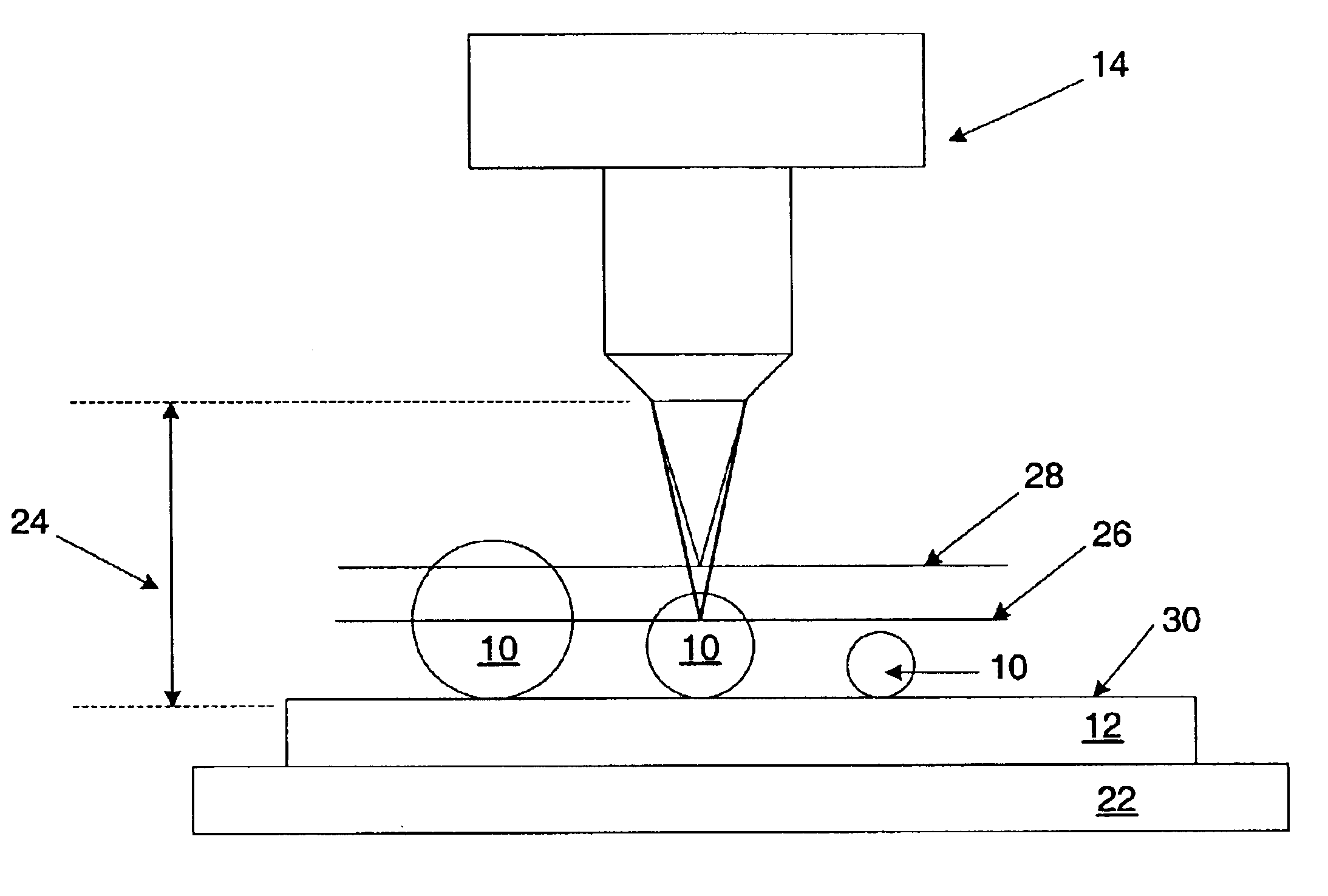
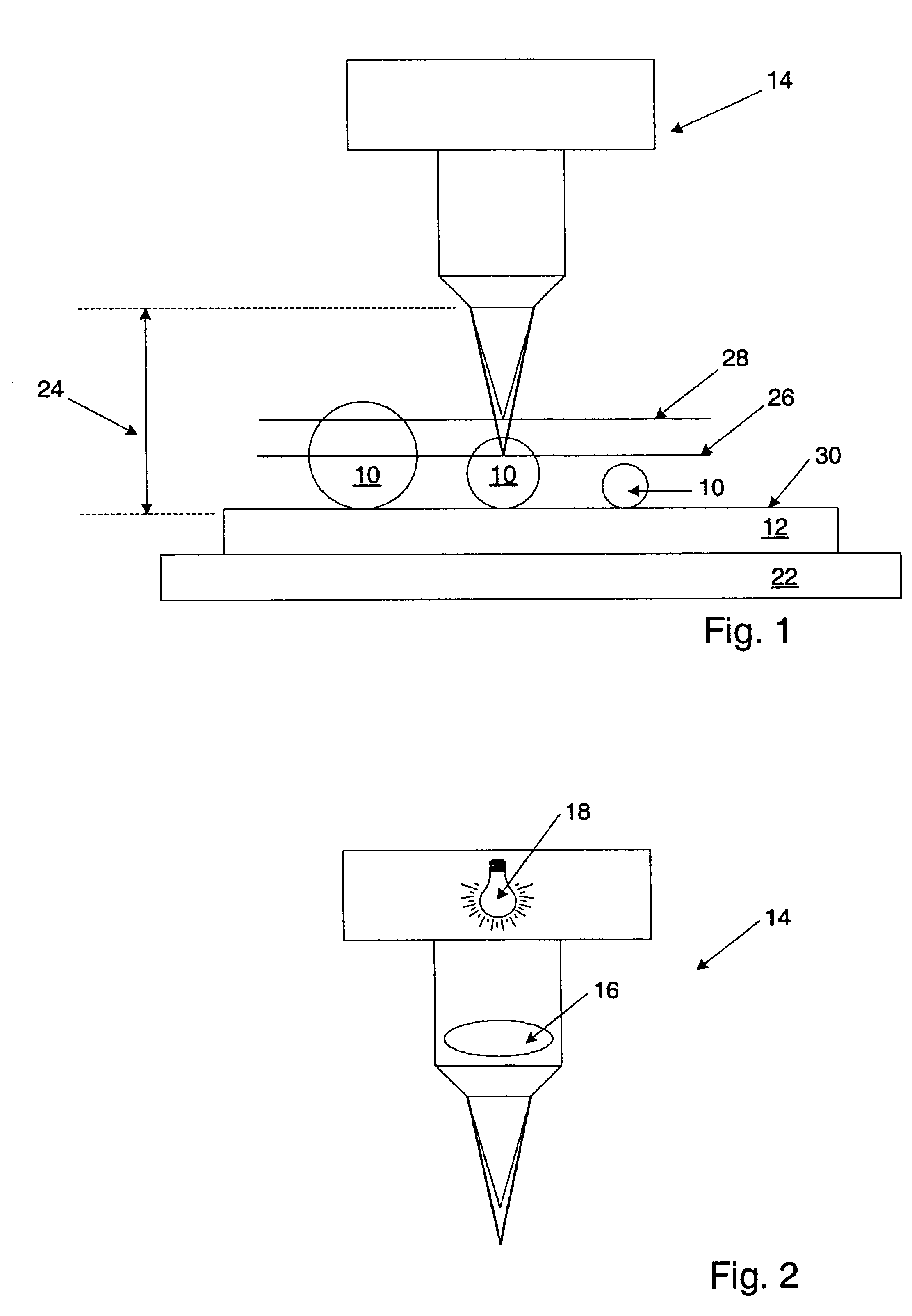
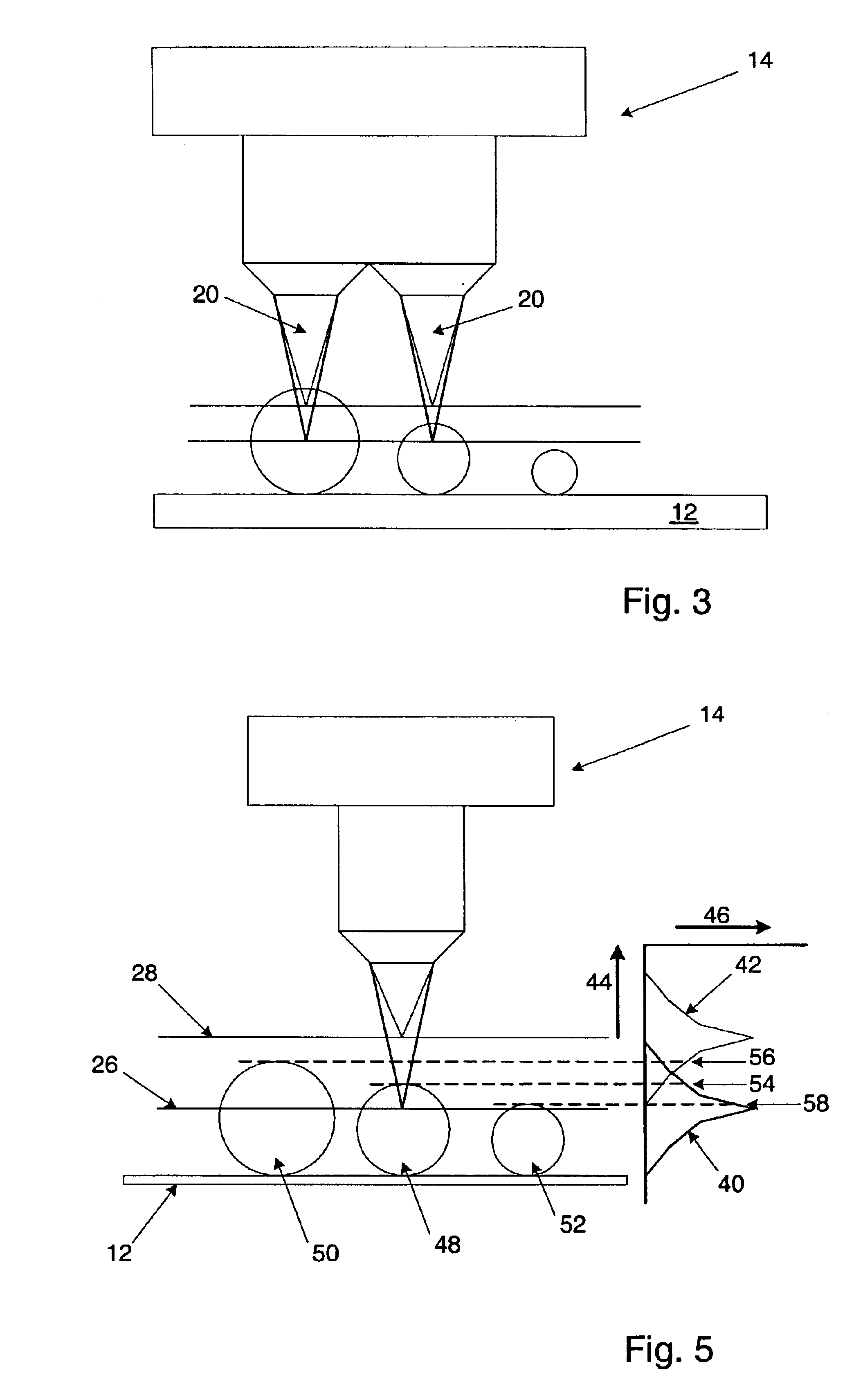
[0032]FIG. 1 illustrates a partial schematic side view of a system configured to assess a dimension of feature 10 on specimen 12. Feature 10 may include, but is not limited to, a bump. As described herein, a bump may be a relatively small solder ball that may be used to couple a semiconductor device to a chip carrier. A bump, however, may also include gold bumps, solder paste bumps, or any other bumps known in the art. Specimen 12 may be a wafer. A wafer may include a monocrystalline silicon substrate suitable for the fabrication of semiconductor devices. In this manner, specimen 12 may be commonly referred to as a “bumped-wafer.” The specimen may also include a wafer produced by wafer-level packaging processes such as, but not limited to, UltraCSP® available from Kulicke & Soffa Flip Chip Division, Phoenix, Ari., wCSP available from Integrated Electronics and Packaging Technologies, Inc. (Casio / Oki), Hachioji, Japan, and Super CSP™ available from Fujitsu Microelectronics America, I...


PUM


Abstract

Systems and methods for assessing a dimension of a feature on a specimen are provided. A system may include an illumination system configured to scan the specimen with light at multiple focal planes substantially simultaneously. The system may also include a collection system that may include multiple collectors. Approximately all light returned from one of the multiple focal planes may be collected by one of the multiple collectors. In addition, the system may include a processor configured to determine a relative intensity of the collected light. The processor may also be configured to assess a dimension of the feature on the specimen in a direction substantially perpendicular to an upper surface of the specimen using the relative intensity.

Description

PRIORITY CLAIM[0001]This application claims priority to U.S. Provisional Application No. 60 / 329,034 entitled “Systems and Methods for Three-Dimensional Inspection and / or Metrology of a Specimen,” filed Oct. 12, 2001.BACKGROUND OF THE INVENTION[0002]1. Field of the Invention[0003]The present invention generally relates to systems and methods for three-dimensional inspection and / or metrology of a specimen. Certain embodiments relate to systems and methods for inspecting a specimen such as a bumped wafer with laser scanning chromatic confocal microscopy.[0004]2. Description of the Relevant Art[0005]Fabricating semiconductor devices such as logic and memory devices may typically include processing a specimen such as a wafer using a number of semiconductor fabrication processes to form various features and multiple levels of the semiconductor devices. For example, lithography is a semiconductor fabrication process that typically involves transferring a pattern to a resist arranged on a w...

Claims


Application Information

Patent Timeline
IPC IPC(8): G01N21/00G01B11/06G01N21/95
CPCG01B11/0608G01N21/9501
Inventor WIHL, TIMHIEBERT, STEPHENSCHMIDLEY, RICHARD
Owner KLA TENCOR TECH CORP
Why Eureka
Try Eureka