Thin film magnetic memory device storing program information efficiently and stably

a program information and stably storage technology, applied in the direction of static storage, digital storage, instruments, etc., can solve the problems of data once programmed being rewritten, enormous time and cost spent on the programming process, and data rewriting. , to achieve the effect of efficient and stable storage of program information

Inactive Publication Date: 2005-07-12
RENESAS ELECTRONICS CORP
View PDF7 Cites 27 Cited by
  • Summary
  • Abstract
  • Description
  • Claims
  • Application Information

AI Technical Summary

Benefits of technology

[0012]The present invention has been made to solve the above-described problems. An object of the present invention is to provide a configuration of thin film magne

Problems solved by technology

As the configuration required special equipment such as a trimming device dedicated to laser blowing, enormous time and cost were spent for the programming process.
Thus, once a memory device is packaged as a final product after defective addresses corresponding to defective memory cells detected at the wafer level have been programmed, it would be difficult to remedy any defects that occur to the

Method used


Image

  • Thin film magnetic memory device storing program information efficiently and stably
  • Thin film magnetic memory device storing program information efficiently and stably
  • Thin film magnetic memory device storing program information efficiently and stably

Examples


first embodiment

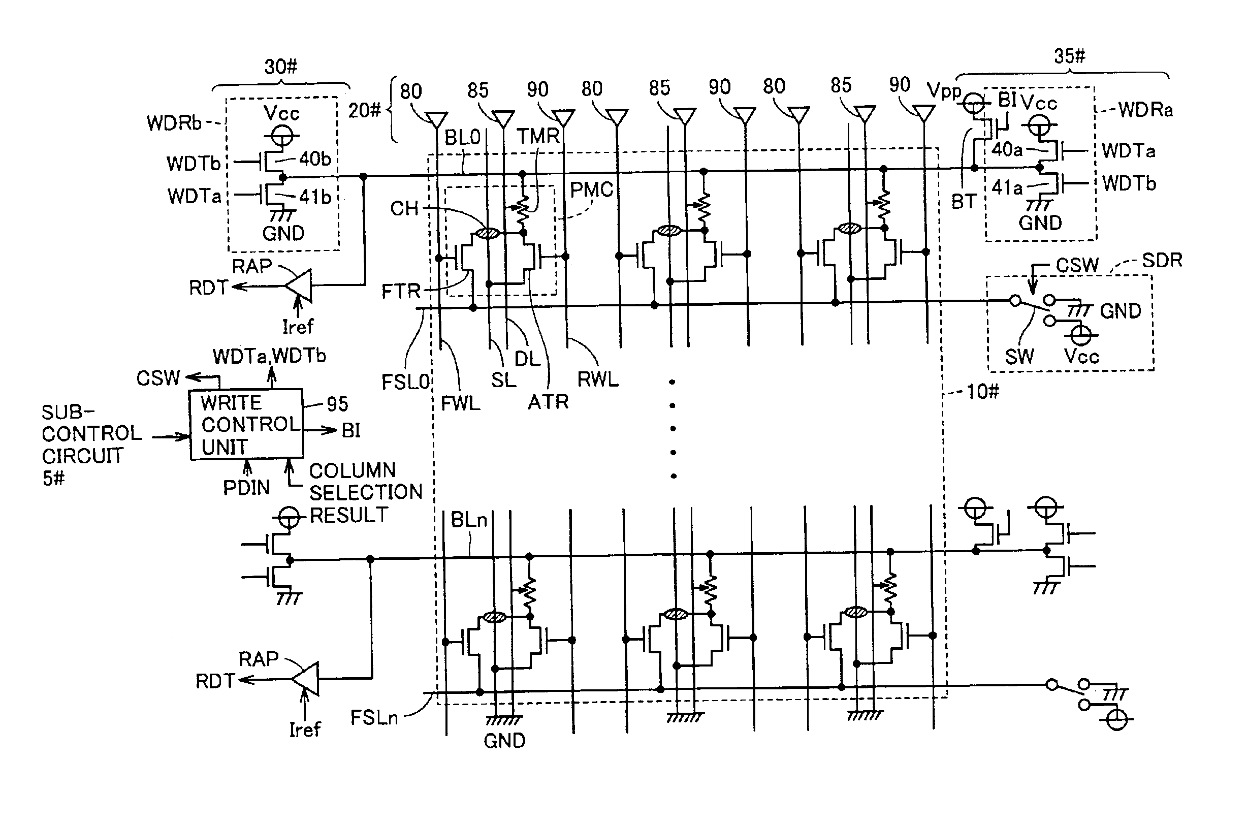
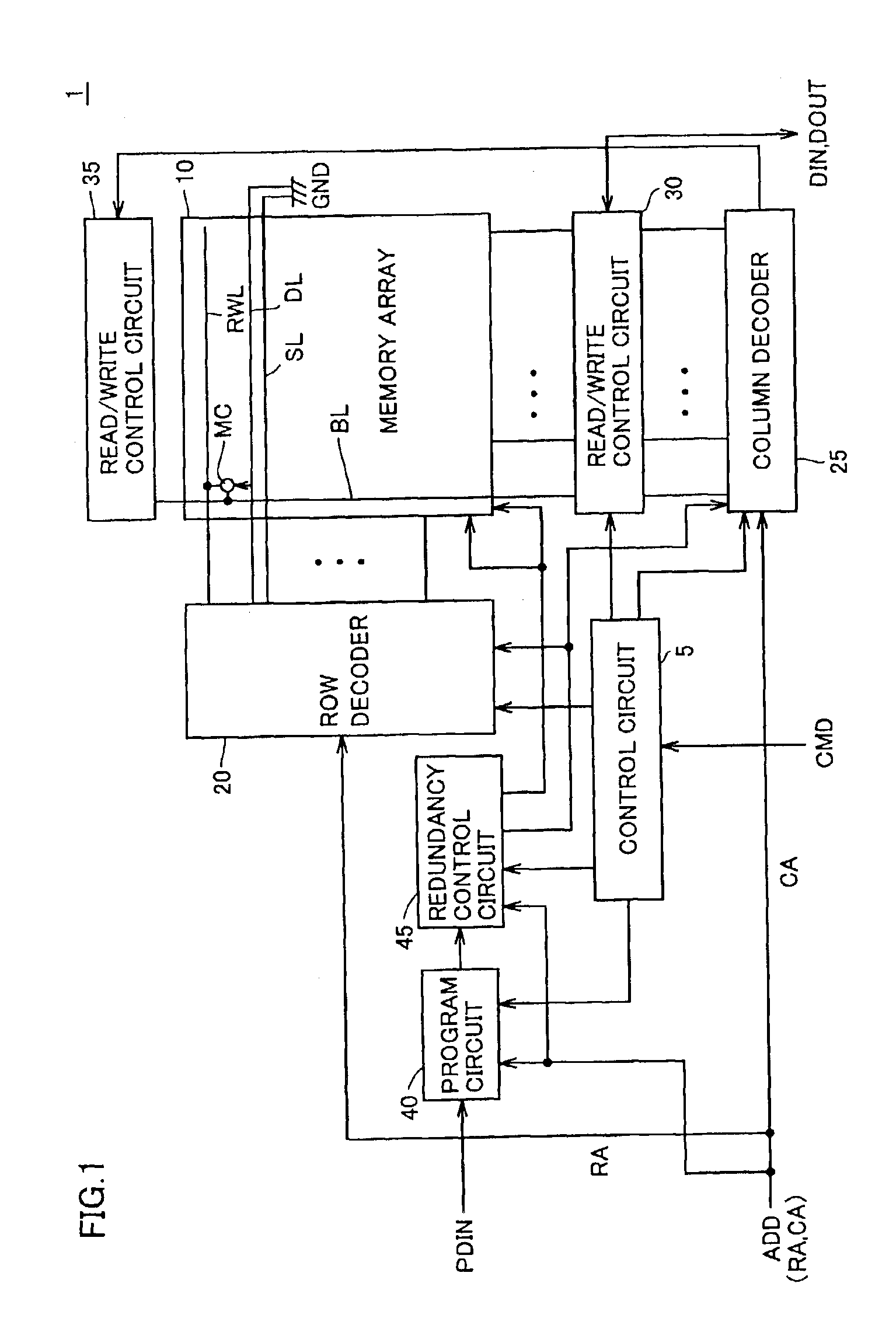
[0049]Referring to FIG. 1, the MRAM device 1 according to an embodiment of the present invention performs random access in accordance with a control signal CMD and an address signal ADD supplied externally, and performs input of write data DIN and output of read data DOUT.

[0050]MRAM device 1 is provided with a control circuit 5 for controlling the entire operation of MRAM device 1 in accordance with control signal CMD, and a memory array 10 having a plurality of MTJ memory cells arranged in rows and columns. Memory array 10 includes a plurality of normal MTJ memory cells arranged in rows and columns, each addressable by address signal ADD, and spare memory cells (not shown) for replacement of defective normal memory cells. In memory array 10, word lines, digit lines and source lines are arranged corresponding to respective memory cell rows, and bit lines are arranged corresponding to respective memory cell columns.

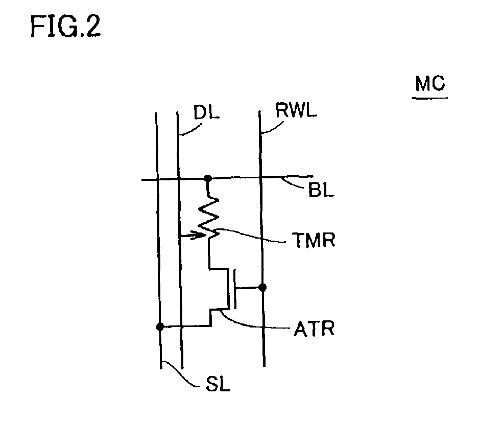
[0051]In FIG. 1, one memory cell MC is shown in memory array 10, and ...

second embodiment

[0148]In the first embodiment above, the configuration of program circuit 40 having integrally arranged memory cells PMC capable of efficiently storing program data has been described.

[0149]In the second embodiment of the present invention, a program circuit configured with a program element automatically decoding program data upon power-up is described.

[0150]Referring to FIG. 16, a program unit PMU constituting the program element according to the second embodiment includes: a bit line SBL for supplying a data write current; bit line drivers WWRb, WWRa provided corresponding to one end and the other end of bit line SBL; a program cell unit PMCUb provided on the one end of bit line SBL and electrically coupled to bit line SBL and storing program data; a program cell unit PMCUa provided on the other end of bit line SBL and storing program data; and a write / read control unit 140 generating write control signals WDTa, WDTb and control signals DA, / DA in response to program data PDIN ex...

third embodiment

[0208]In the third embodiment of the present invention, application of program unit PMU in the second embodiment to a system employing a field programmable gate array (FPGA) is explained. The FPGA is a semiconductor device which has an internal circuit provided therein in advance and which can be changed to perform a prescribed operation by externally providing data and others to the internal circuit afterward. Generally, the program information for use in such a change of the operation is stored in a prescribed region within the internal circuit.

[0209]Referring to FIG. 27, the FPGA according to the third embodiment includes a plurality of circuit blocks BK arranged in rows and columns, and interconnection regions are provided between these blocks. In the interconnection regions, a plurality of horizontal interconnection groups XG and a plurality of vertical interconnection groups YG are provided in a row direction and in a column direction, respectively.

[0210]Each of circuit blocks...


PUM


Abstract

Each of program cell and memory cells includes a magnetic storage portion of the same configuration. The program cell further includes a state change portion. That is, the program cell has the same structure as the memory cell, except that the state change portion is additionally provided thereto. As such, the program cell can be provided efficiently, as it can be designed the same as the memory cell in terms of the magnetic storage portion and others. The state change portion makes a transition to a fixed state based on an electrical change. Thus, the state change portion prevents program information from being rewritten by a magnetic noise or the like, and ensures stable storage of the program information.

Description

BACKGROUND OF THE INVENTION[0001]1. Field of the Invention[0002]The present invention relates to thin film magnetic memory devices, and more particularly to a thin film magnetic memory device provided with memory cells having magnetic tunnel junctions (MTJ) (hereinafter, also simply referred to as the “MTJ memory cells”).[0003]2. Description of the Background Art[0004]In recent years, a magnetic random access memory (MRAM) device has attracted attention as a next-generation nonvolatile memory device. The MRAM device stores data in a non-volatile manner using a plurality of thin film magnetic elements formed in a semiconductor integrated circuit, and permits random access to the respective thin film magnetic element.[0005]In particular, recent announcement shows that the performance of the MRAM device is significantly improved by using thin film magnetic elements utilizing the magnetic tunnel junctions as memory cells.[0006]It is common in memory devices to perform normal operations ...

Claims


Application Information

Patent Timeline
IPC IPC(8): G11C11/15G11C11/02G11C16/06G11C29/04G11C29/12
CPCG11C11/15G11C11/16G11C11/5607
Inventor OOISHI, TSUKASA
Owner RENESAS ELECTRONICS CORP
Why Eureka
Try Eureka