64-bit single cycle fetch scheme for megastar architecture

Active Publication Date: 2005-07-12
TEXAS INSTR INC
View PDF3 Cites 1 Cited by
  • Summary
  • Abstract
  • Description
  • Claims
  • Application Information

AI Technical Summary

Benefits of technology

[0008]This invention describes a hardware approach allowing a 64-bit fetch from memory on one clock cycle for the ‘megastar’ processor core. The ‘megastar’ core incorporates 32-bit word memory units broken out into separate ‘entities’ or ‘banks’. However, the host processor chip itself has only three 16-bit read buses. This means that the maximum read that can be done in one clock cycle is 48-bits. In certain applications, such as the digital audio floating-point accelerator for exam

Problems solved by technology

However, the host processor chip its

Method used


Image

  • 64-bit single cycle fetch scheme for megastar architecture
  • 64-bit single cycle fetch scheme for megastar architecture
  • 64-bit single cycle fetch scheme for megastar architecture

Examples


Embodiment Construction

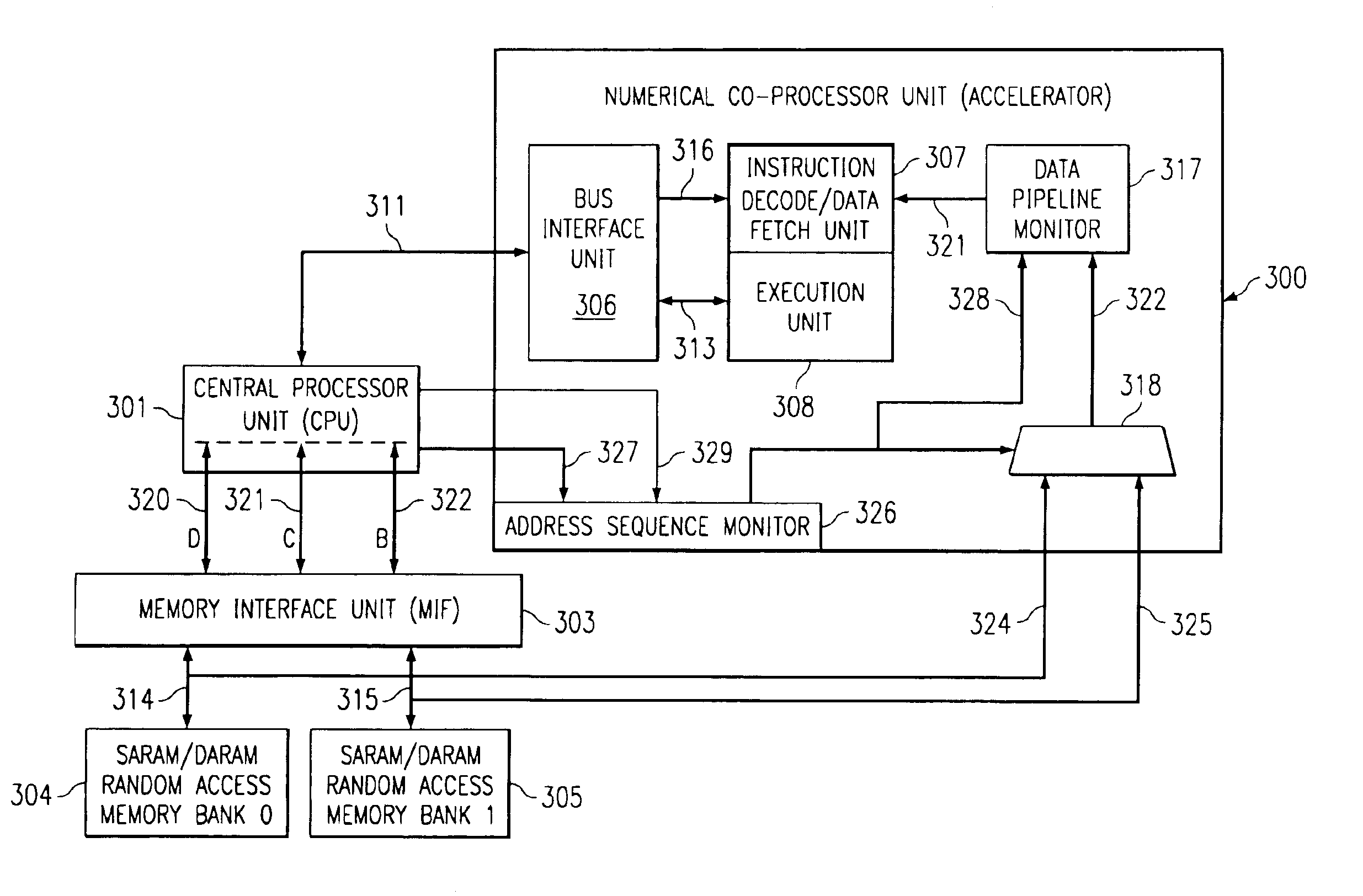
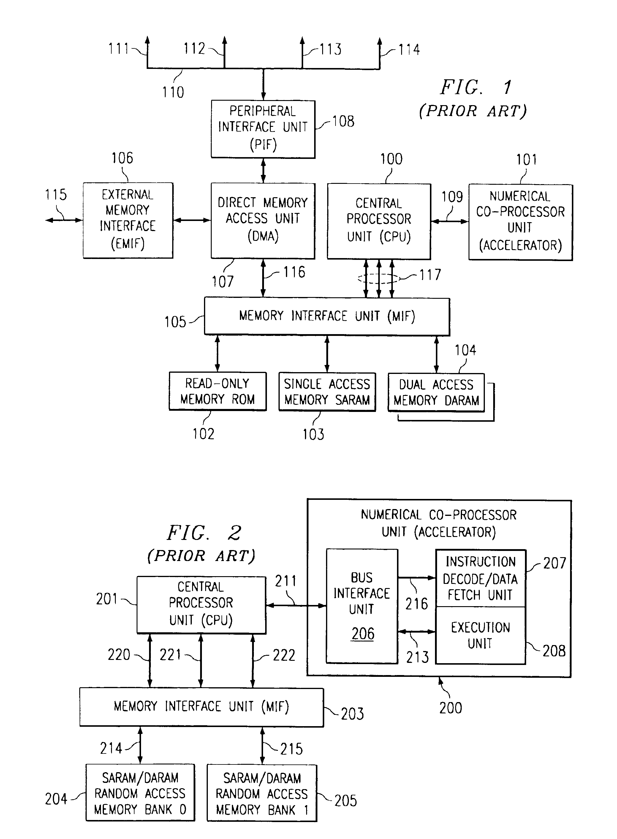
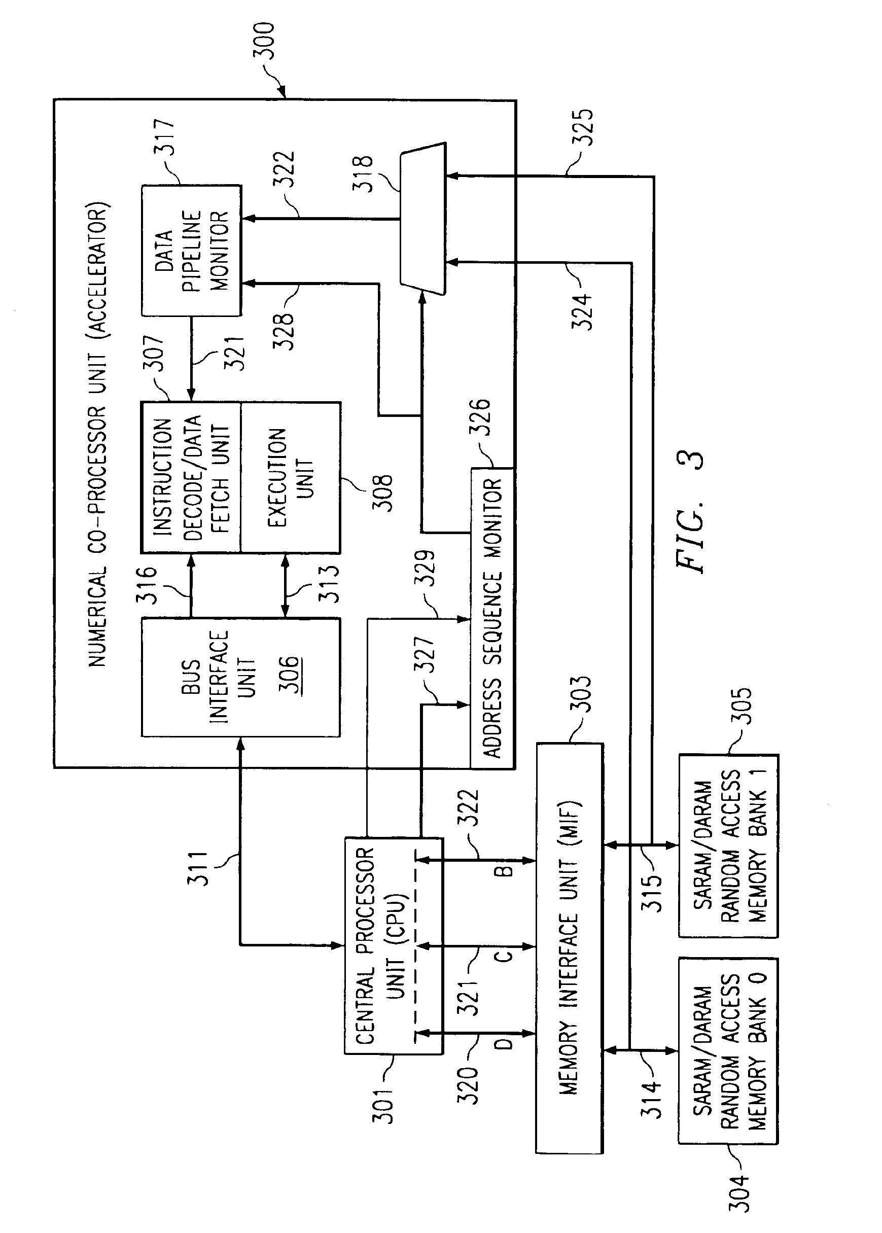
[0013]The 64-bit single cycle fetch method of this invention is illustrated in FIG. 3. The CPU 301 is programmed to fetch 48-bits through memory interface unit (MIF) 303. This fetch is accomplished in busses 320, 321 and 322, composite busses containing address, data and control signals. The CPU sends addresses over these three busses and receives ‘read’ data in return. Memory is organized as 32-bit wide data banks, illustrated as combined SARAM and DARAM banks in FIG. 2 by Bank-0304, and Bank-1305. Memory bank-0304 is connected to MIF 303 via bus 314. Memory bank-1305 is connected to MIF 303 via 315. The 48-bits of data fetched by the CPU is passed to the numerical co-processor unit via path 311 through the bus interface unit 306 and on to the instruction decode / data fetch unit 307 via path 316. The present invention describes the method by which an additional 16-bits of fetched data is retrieved through path 321 from the data pipeline monitor 317.

[0014]Because memory in the megast...


PUM


Abstract

The 64-bit single cycle fetch method described here relates to a specific ‘megastar’ core processor employed in a range of new digital signal processor devices. The ‘megastar’ core incorporates 32-bit memory blocks arranged into separate entities or banks. Because the parent CPU has only three 16-bit buses, a maximum read in one clock cycle through the memory interface would normally be 48-bits. This invention describes an approach for a fetch method involving tapping into the memory bank data at an earlier stage prior to the memory interface. This allows the normal 48-bit fetch to be extended to 64-bits as required for full performance of the numerical processor accelerator and other speed critical operations and functions.

Description

TECHNICAL FIELD OF THE INVENTION[0001]The technical field of this invention is computer architecture and more particularly data movement in computer systems.BACKGROUND OF THE INVENTION[0002]The basic architecture of a wide range of digital signal processors having embedded numerical processor accelerators has been labeled the ‘megastar’ architecture. FIG. 1 illustrates the block diagram of the ‘megastar’ architecture. The central processor unit 100 is linked by busses 117 to internal memory including ROM 102, single-access SARAM 103, and dual-access DARAM 104 by way of memory interface unit (MIF) 105. MIF also links the processor and internal memory to external memory bus 115 via DMA 107 and external memory interface 106. The peripheral interface unit (PIF) 108 provides a bus 110 to a number of external peripherals as denoted by ports 111, 112, 113 and 114.[0003]The numerical co-processor unit 101 communicates exclusively with the main CPU 100 via bus 109. This numerical co-processo...

Claims


Application Information

Patent Timeline
IPC IPC(8): G06F12/00G06F9/38
CPCG06F9/3816G06F9/3824G06F9/383
Inventor SAMUEL, ROSHAN J.KRIDNER, JASON D.
Owner TEXAS INSTR INC
Why Eureka
Try Eureka