High speed interface device for reducing power consumption, circuit area and transmitting/receiving a 4 bit data in one clock period

a high-speed interface and clock period technology, applied in the direction of digital transmission, generating/distributing signals, instruments, etc., can solve the problems of increasing power consumption of driver circuits, difficult to use direct rambus dram or sync link dram in all memory products, etc., to improve data i/o efficiency, improve data synchronization, and improve data synchronization efficiency

Inactive Publication Date: 2005-07-12
SK HYNIX INC
View PDF5 Cites 15 Cited by
  • Summary
  • Abstract
  • Description
  • Claims
  • Application Information

AI Technical Summary

Benefits of technology

[0012]The claimed inventions feature at least in part a high speed interface device which can improve data I / O efficiency by increasing data outputted in one period in an SDRAM, by four times, and which can provide a bus structure for enabling more precise synchronization of a data and a clock in the high speed operation.

Problems solved by technology

It is thus difficult to use a direct Rambus DRAM or sync link DRAM in all memory products.
Moreover, the driver circuits increase power consumption.

Method used


Image

  • High speed interface device for reducing power consumption, circuit area and transmitting/receiving a 4 bit data in one clock period
  • High speed interface device for reducing power consumption, circuit area and transmitting/receiving a 4 bit data in one clock period
  • High speed interface device for reducing power consumption, circuit area and transmitting/receiving a 4 bit data in one clock period

Examples


Embodiment Construction

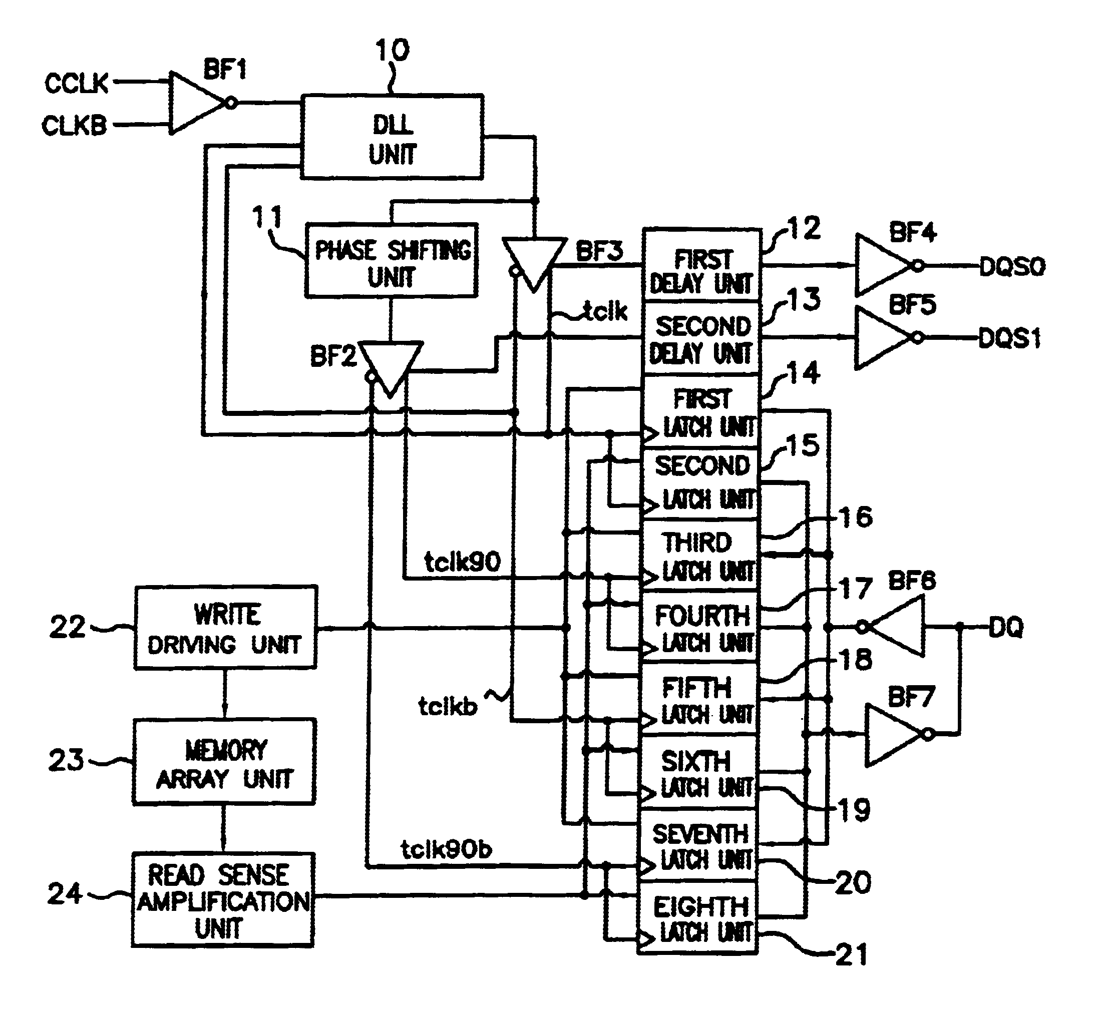
[0023]A high speed interface device in accordance with a preferred embodiment of the present invention will now be described in detail with reference to the accompanying drawings. Elements having an identical or similar function are provided with the identical reference numeral, and repeated explanations thereof will be omitted.

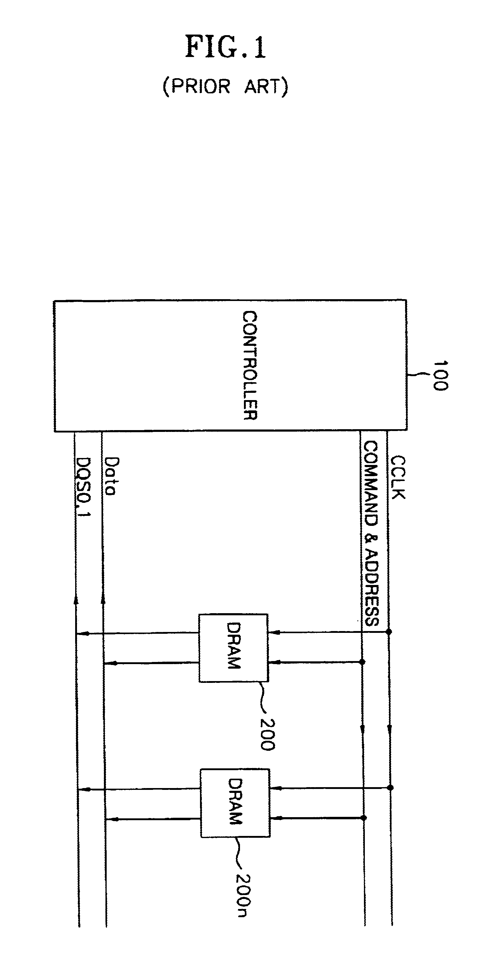
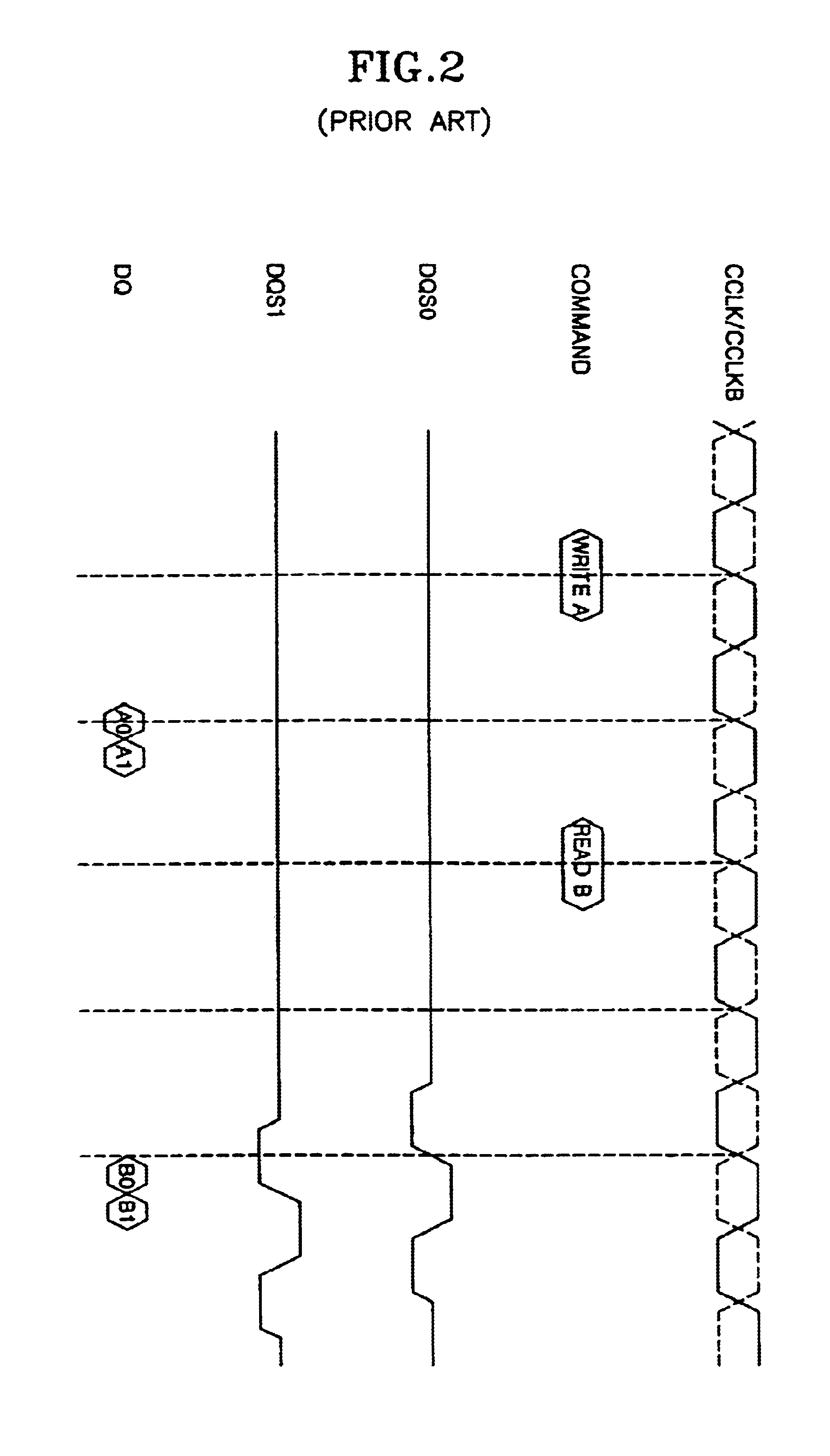
[0024]FIG. 3 is a timing diagram illustrating a data I / O in read and write operations in the high speed interface type device in accordance with the present invention. The high speed interface type device will now be explained with reference to FIG. 3 and the system bus structure of the conventional interface type device in FIG. 1 (Prior Art).

[0025]When the respective DRAMs 200˜200n receive a clock signal CCLK from a controller 100, and then receive a write command signal WRITE A, the DRAMs 200˜200n receive a write data signal synchronized with the clock signal CCLK from the controller 100. The write data signal inputted to the DRAMs 200˜200n is a 4 bit write...


PUM


Abstract

A high speed interface type device can reduce power consumption and a circuit area, and transmit/receive a 4 bit data in one clock period. The high speed interface type device includes a DRAM unit for generating first clock and clock bar signals which do not have a phase difference from a main clock signal, and second clock and clock bar signals having 90° phase difference from the first clock and clock bar signals in a write operation, storing an inputted 4 bit data in one period of the main clock signal according to the first clock to second clock bar signals, synchronizing the stored data with data strobe signals according to the first clock to second clock bar signals in a read operation, and outputting a 4 bit data in one period of the main clock signal, and a controller for transmitting a command, address signal and data signal synchronized with the main clock signal to the DRAM unit in the write operation, and receiving data signals from the DRAM unit in the read operation.

Description

BACKGROUND OF THE INVENTION[0001]1. Field of the Invention[0002]The present invention relates in general to a high speed interface device, and in particular to an improved high speed interface type device which can improve data I / O efficiency by increasing data output in one period in an SDRAM, by four times, and which can provide a bus structure for enabling more precise synchronization of a data and a clock during high speed operation.[0003]2. General Background and Related Art[0004]In general, a high speed DRAM such as a direct Rambus DRAM or sync link DRAM has a higher data processing speed than a conventional DRAM. Accordingly, the direct Rambus DRAM or sync link DRAM must be used in consideration of a data processing speed of peripheral systems. It is thus difficult to use a direct Rambus DRAM or sync link DRAM in all memory products. Therefore, it is required to develop a high speed DRAM by gradually improving the existing DRAM. Recently, many companies have attempted to desi...

Claims


Application Information

Patent Timeline
Patent Type & Authority Patents(United States)
IPC IPC(8): G11C7/00G11C7/10G11C7/22G11C11/4093G11C11/409G11C11/4076G11C11/407G11C11/413
CPCG11C7/1072G11C7/22G11C7/222G11C11/4076G11C11/4093G11C11/413
Inventor PARK, YONG JAEJOO, JONG DOO
Owner SK HYNIX INC
Why Eureka
Try Eureka