Double diffused field effect transistor having reduced on-resistance

a field effect transistor and on-resistance technology, applied in the field of semiconductor wafer processing, can solve the problems of high energy ion implantation techniques, unsatisfactory decrease of device breakdown voltage, and additional masking steps

Inactive Publication Date: 2005-07-26
GEN SEMICON
View PDF8 Cites 0 Cited by
  • Summary
  • Abstract
  • Description
  • Claims
  • Application Information

AI Technical Summary

Problems solved by technology

Since the magnitude of the on-resistance and the breakdown voltage vary in a similar manner with respect to dopant concentration, decreasing the on-resistance of a double diffused field effect transistor by increasing the doping concentration in the epitaxial region 1A causes an undesirable decrease in the breakdown voltage of the device.
On problem with this technique is that it requires additional masking steps and high energy ion implantation techniques to form the localized doping region.

Method used


Image

  • Double diffused field effect transistor having reduced on-resistance
  • Double diffused field effect transistor having reduced on-resistance
  • Double diffused field effect transistor having reduced on-resistance

Examples


Embodiment Construction

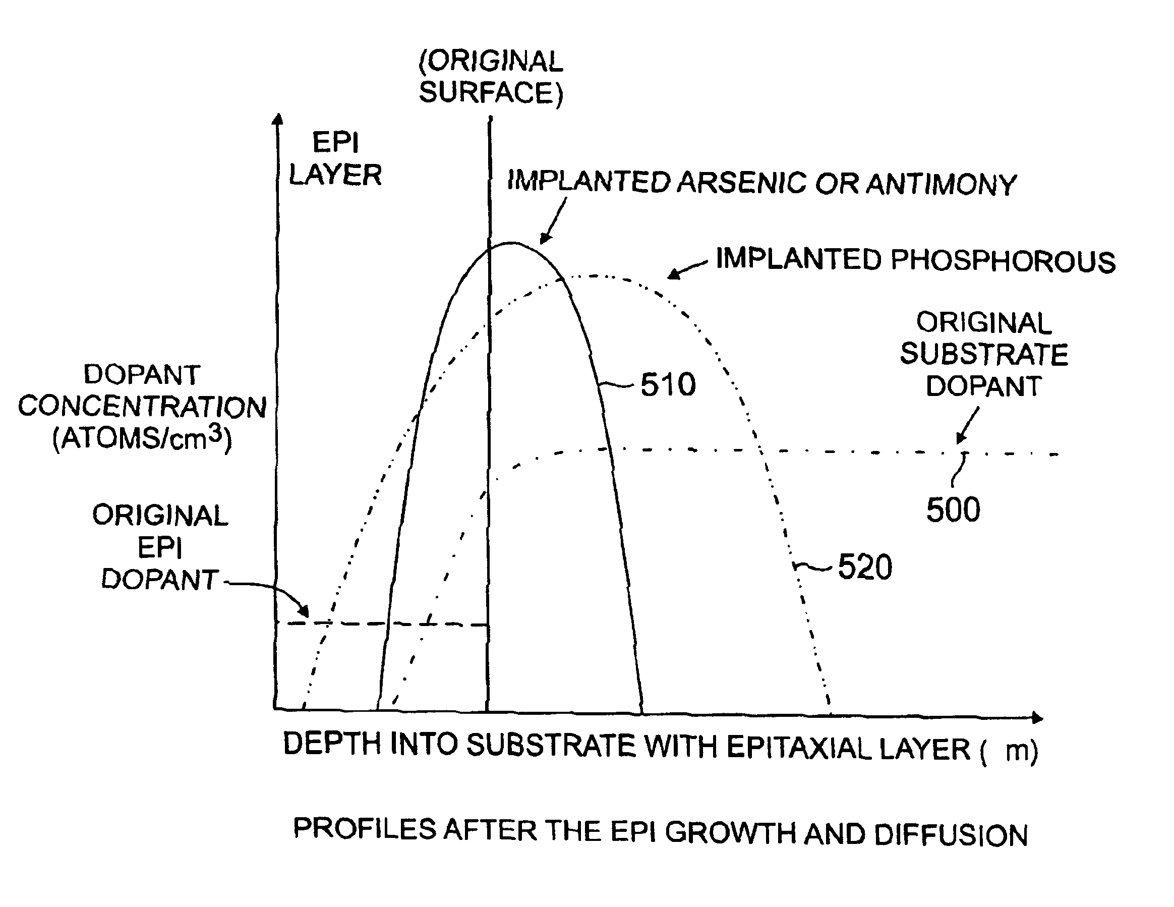
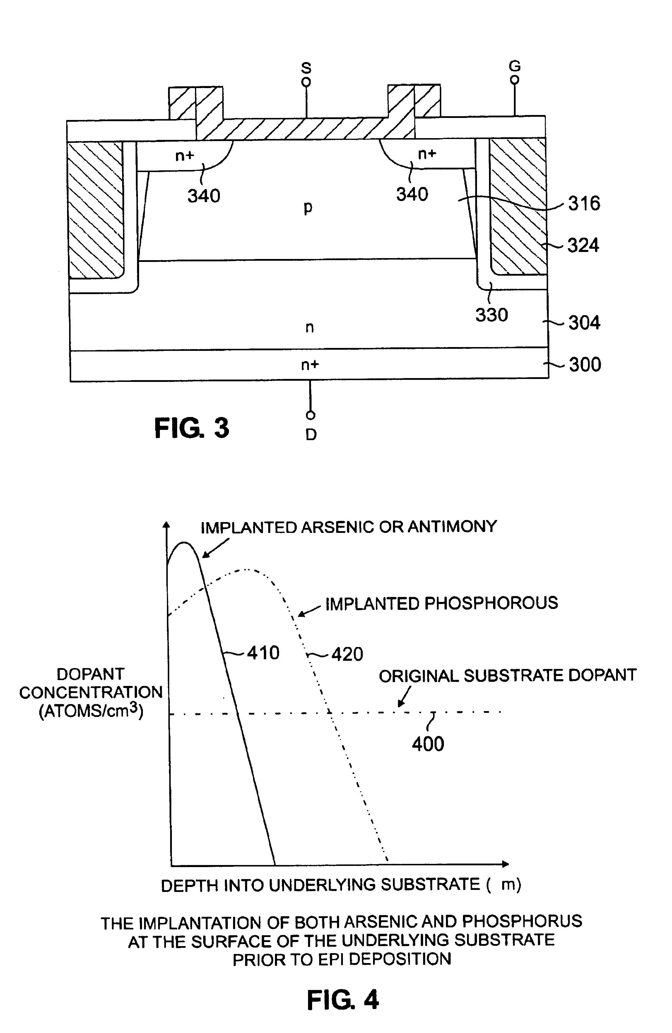
[0023]FIG. 3 illustrates one embodiment of a trench field effect transistor constructed in accordance with the present invention. The structure includes, in this embodiment, an n+ substrate 300 on which is grown a lightly n-doped epitaxial layer 304. As described in more detail below, the surface region of substrate 300 has a higher dopant concentration than its interior. Within doped epitaxial layer 304, a body region 316 of opposite conductivity is provided. An n+-doped region 340 that overlies most of the body region 316 serves as the source. A rectangular shaped trench 324 is provided in the epitaxial layers, which is open at the upper surface of the structure and defines the perimeter of the transistor cell. A gate oxide layer 330 lines the sidewalls of the trench 324. The trench 324 is filled with polysilicon, i.e., polycrystalline silicon that has been doped to make it conductive. A drain electrode is connected to the back surface of the semiconductor substrate 300, a source ...


PUM


Abstract

A double diffused field effect transistor and a method of forming the same is provided. The method begins by providing a substrate of a first conductivity type. Next, at least one dopant species, also of the first conductivity type, is introduced into a surface of the substrate so that the substrate has a nonuniform doping profile. An epitaxial layer of the first conductivity type is formed over the substrate and one or more body regions of a second conductivity type are formed within the epitaxial layer. A plurality of source regions of the first conductivity type are then formed within the body regions. Finally, a gate region is formed, which is adjacent to the body regions.

Description

STATEMENT OF RELATED APPLICATION[0001]This application is a divisional of U.S. patent application Ser. No. 09 / 819,356, filed Mar. 28, 2001 now U.S. Pat. No. 6,713,351, entitled “Double Diffused Field Effect Transistor Having Reduced On-Resistance,” which is incorporated by reference in its entirety herein.FIELD OF THE INVENTION[0002]This invention relates generally to semiconductor wafer processing and more particularly to a method for forming a double diffused field effect transistor.BACKGROUND INFORMATION[0003]Power MOSFET devices are well known and are used in many applications including automotive electronics, portable electronics, power supplies, and telecommunications. One important electrical characteristic of a power MOSFET device is its on-state resistance (RDSon), which is defined as the total resistance encountered by the carriers as they flow from the source terminal to the drain terminal. In order to allow manufacturers to produce power MOSFET devices having higher curr...

Claims


Application Information

Patent Timeline
Patent Type & Authority Patents(United States)
IPC IPC(8): H01L21/336H01L29/78H01L21/02H01L29/66H01L29/08H01L29/02
CPCH01L29/0878H01L29/7813H01L29/78
Inventor BLANCHARD, RICHARD A.
Owner GEN SEMICON
Why Eureka
Try Eureka