Radio frequency lateral double diffused field effect transistor and its manufacturing method

A technology of field-effect transistors and lateral double diffusion, which is applied in semiconductor/solid-state device manufacturing, semiconductor devices, electrical components, etc., to achieve the effect of reducing on-resistance and high breakdown voltage

Active Publication Date: 2016-04-13
SHANGHAI HUAHONG GRACE SEMICON MFG CORP
View PDF3 Cites 0 Cited by
  • Summary
  • Abstract
  • Description
  • Claims
  • Application Information

AI Technical Summary

Problems solved by technology

However, it is still difficult to achieve a higher breakdown voltage BV (for example, higher than 120V) with only two layers of Faraday shield structure

Method used


Image

  • Radio frequency lateral double diffused field effect transistor and its manufacturing method
  • Radio frequency lateral double diffused field effect transistor and its manufacturing method
  • Radio frequency lateral double diffused field effect transistor and its manufacturing method

Examples


Embodiment Construction

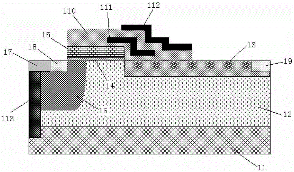
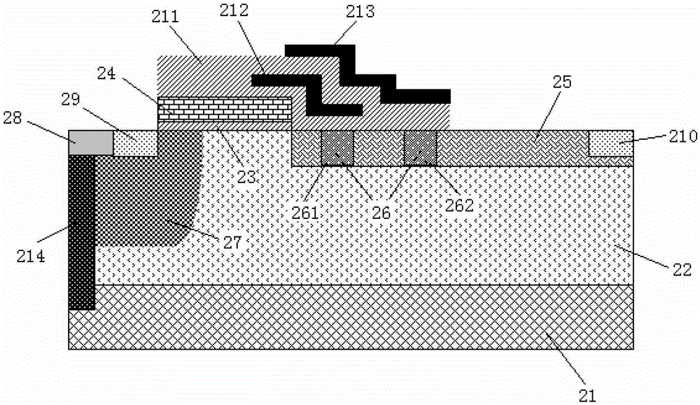
[0056] Such as figure 2As shown, the RFLDMOS device structure of the present invention includes growing a P-type epitaxial layer 22 on the P-type substrate 21, growing a layer of gate oxide layer 23 by thermal oxygen; depositing polysilicon, and defining and etching the polysilicon by a photolithography plate gate 24; then define and perform ion implantation on the P-type epitaxial layer 22 through a photolithography plate to form a lightly doped drift region (NLDD) 25; perform a second doping in the lightly doped drift region 25 to form two The second NLDD implantation region 26, the two second NLDD implantation regions 26 are respectively the implantation region 261 under the first layer of Faraday shield and the implantation region 262 under the second layer of Faraday shield, respectively formed by ion implantation and diffusion processes P well 27, P+ region 28, N+ source region 29 and N+ drain region 210; then deposit a layer of oxide layer 211, deposit metal or metal s...


PUM


Abstract

The invention discloses a radio frequency lateral double-diffusion field effect transistor, which comprises a P-type substrate, a P-type epitaxial layer is grown on the P-type substrate, a lightly doped drift region is formed in the P-type epitaxial layer, and A first layer of Faraday shield and a second layer of Faraday shield are arranged above the P-type epitaxial layer, and two second NLDD implantation regions are also included in the lightly doped drift region, respectively located in the first layer of Faraday shield and below the second layer of the Faraday shield. The invention can obtain performance exceeding that of the device with the original structure, realize higher breakdown voltage (higher than 120V), and reduce the on-resistance of the device with the original structure at the same time. At the same time, the invention also discloses a manufacturing method of the transistor.

Description

technical field [0001] The invention relates to a semiconductor integrated circuit manufacturing device, in particular to a radio frequency lateral double-diffusion field effect transistor, and also relates to a manufacturing method of the transistor. Background technique [0002] Radio Frequency Lateral Double Diffusion Field Effect Transistor (RFLDMOS) device is a new generation of integrated solid microwave power semiconductor product formed by the fusion of semiconductor integrated circuit technology and microwave electronic technology. It has good linearity, high gain, high withstand voltage and high output power. , good thermal stability, high efficiency, good broadband matching performance, easy to integrate with MOS process, etc., and its price is much lower than that of gallium arsenide devices. It is a very competitive power device and is widely used in GSM. PCS, power amplifier of W-CDMA base station, wireless broadcasting and nuclear magnetic resonance etc. [0...

Claims


Application Information

Patent Timeline
Patent Type & Authority Patents(China)
IPC IPC(8): H01L29/78H01L29/06H01L21/336
CPCH01L29/404H01L29/7835H01L29/0847
Inventor 李娟娟慈朋亮钱文生韩峰胡君
Owner SHANGHAI HUAHONG GRACE SEMICON MFG CORP
Why Eureka
Try Eureka