

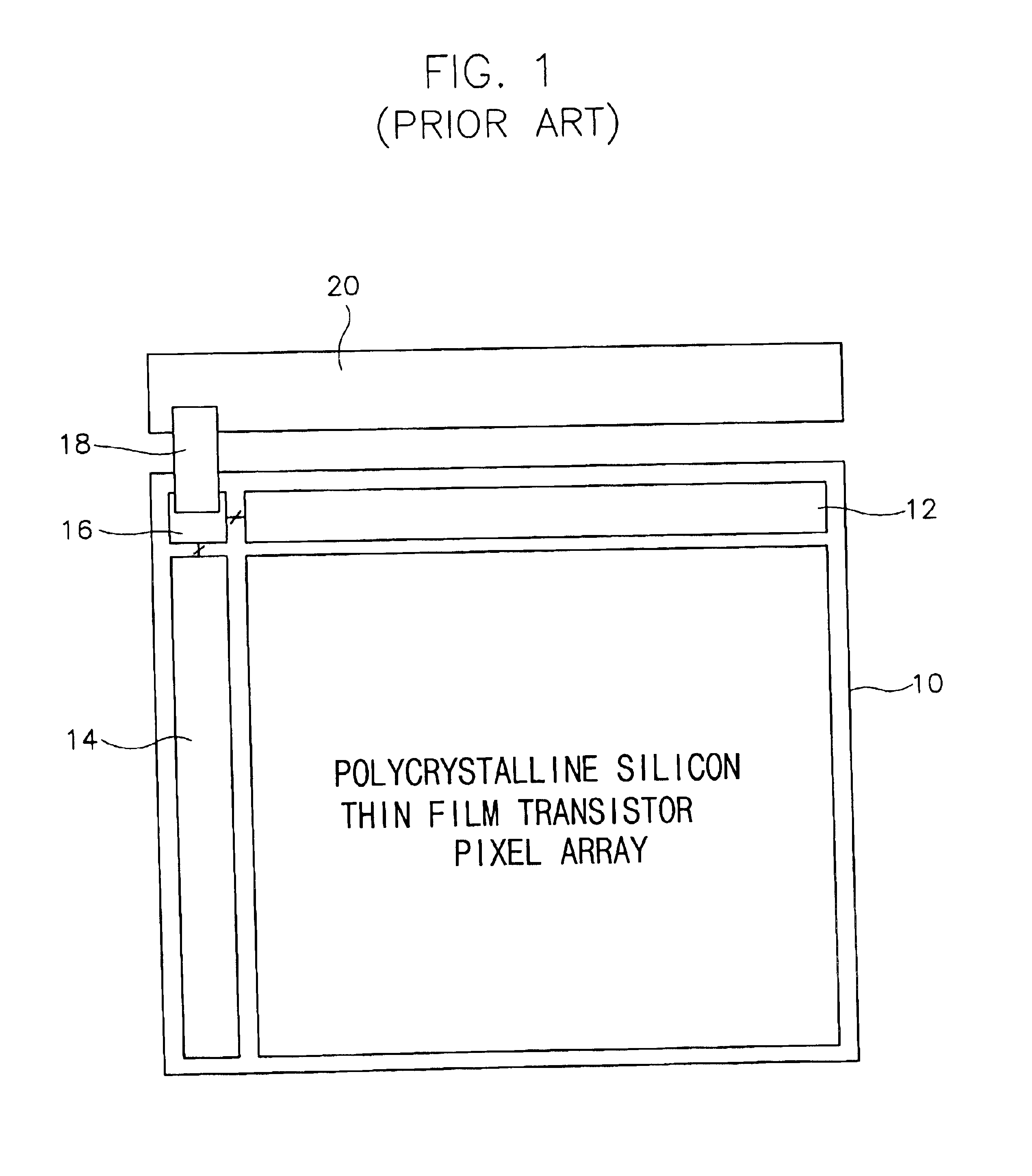
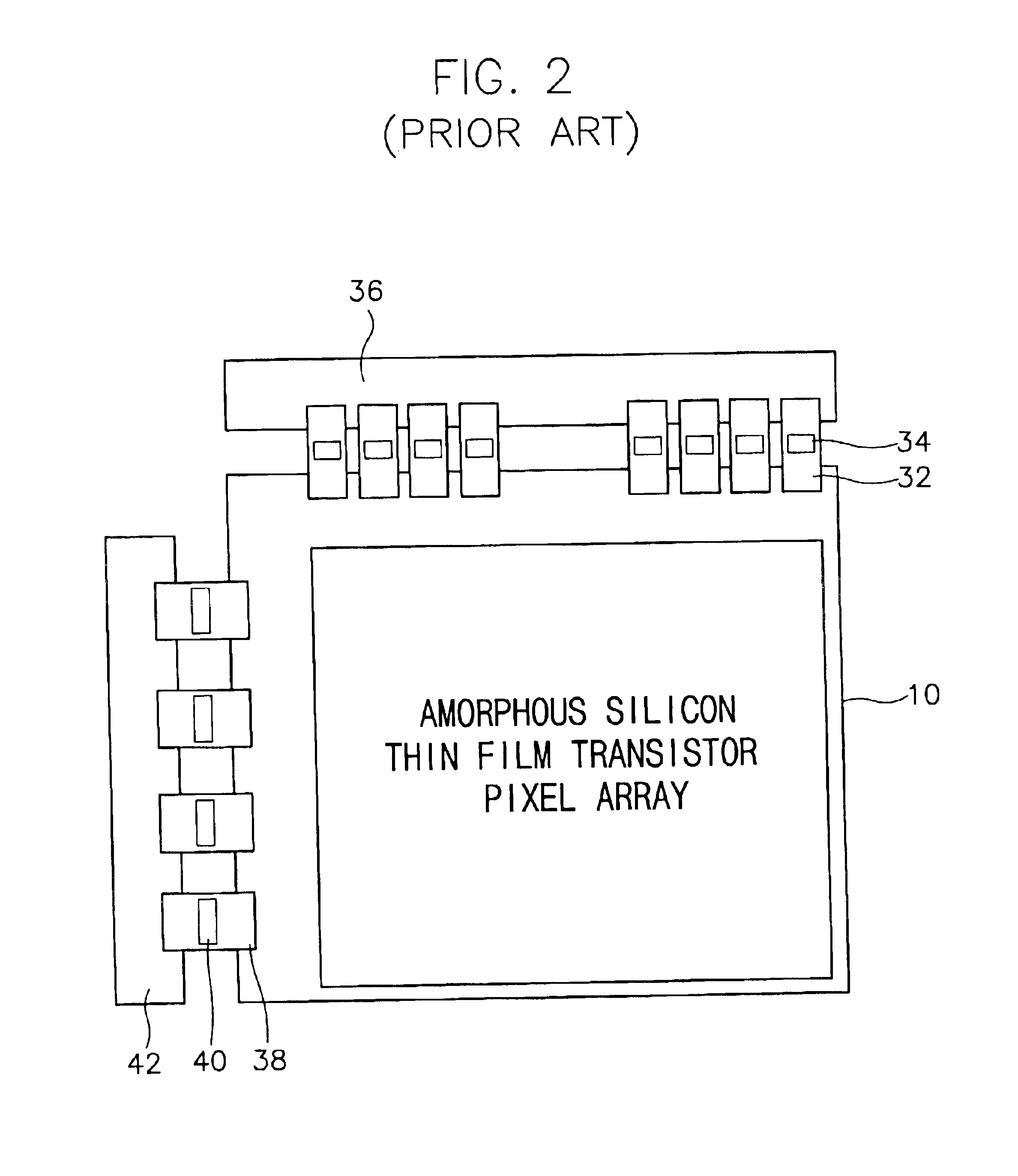
Amorphous silicon thin-film transistor liquid crystal display
a thin film transistor and liquid crystal display technology, applied in static indicating devices, identification means, instruments, etc., can solve the problems of high power dissipation, large volume, heavy weight, etc., and achieve the effect of simplifying the manufacturing process, reducing the number of masks, and reducing the resistance of the main wiring
- Summary
- Abstract
- Description
- Claims
- Application Information
AI Technical Summary
Benefits of technology
Problems solved by technology
Method used
Image

Examples
Embodiment Construction
[0034]For an exemplary amorphous silicon TFT-LCD device type according to an embodiment of the present disclosure, a method is provided whereby the driving circuits and the pixel array are simultaneously formed on a substrate to thereby decrease the number of assembly process steps to a number comparable with that of the polycrystalline silicon TFT-LCD device type. Hereinafter, a preferred embodiment of the present disclosure will be described in detail with reference to the accompanying drawings.
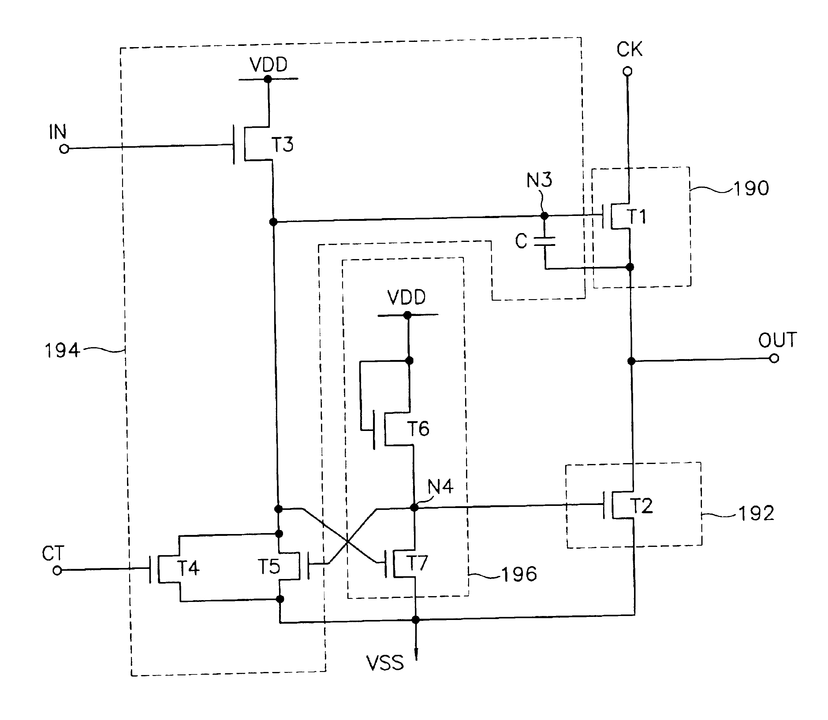
[0035]FIG. 3 is a circuit diagram of a shift register as applied to a gate driving circuit region in an amorphous silicon TFT-LCD device according to an embodiment of the present disclosure. FIG. 4 is a block diagram of a number of interconnected shift registers of FIG. 3.
[0036]Referring to FIGS. 3 and 4, the gate driving circuit has a plurality of shift registers (SR1, SR2, . . . SR93) connected subordinately. That is, an output terminal (“OUT”) of each of the shift registers is connected ...
PUM
| Property | Measurement | Unit |
|---|---|---|
| thickness | aaaaa | aaaaa |
| thickness | aaaaa | aaaaa |
| thickness | aaaaa | aaaaa |
Abstract
Description
Claims
Application Information