DUV scanner linewidth control by mask error factor compensation

a mask and error factor technology, applied in the field of photolithography, can solve the problems of difficult to obtain correct imaging, difficult to correct imaging, and difficult to accurately image and print these small feature sizes on a photosensitive substrate, so as to reduce horizontal and vertical bias in printed features, reduce linewidth variances, and facilitate modification

Inactive Publication Date: 2005-07-26
ASML HLDG NV
View PDF18 Cites 17 Cited by
  • Summary
  • Abstract
  • Description
  • Claims
  • Application Information

AI Technical Summary

Benefits of technology

[0009]It is an advantage of the present invention that it is easily modifiable to accommodate different features to be printed.
[0010]It is a further advantage of the present invention that it reduces linewidth variances in printed features.
[0011]It is yet a further advantage of the present invention that it reduces horizontal and vertical bias in printed features.
[0012]It is a feature of the present invention that an adjustable slit is used to

Problems solved by technology

Correctly imaging and printing these small feature sizes onto a photosensitive substrate becomes increasingly difficult as the feat

Method used


Image

  • DUV scanner linewidth control by mask error factor compensation
  • DUV scanner linewidth control by mask error factor compensation
  • DUV scanner linewidth control by mask error factor compensation

Examples


Embodiment Construction

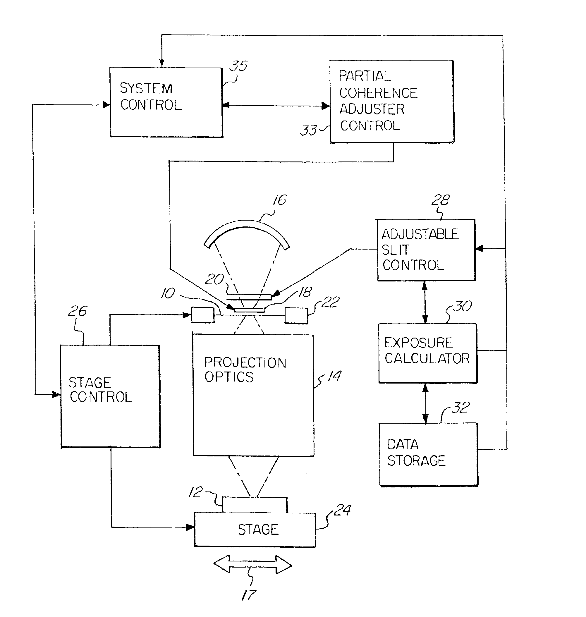
[0034]FIG. 1 schematically illustrates a photolithographic device of the present invention. A mask or reticle 10 having a pattern thereon is imaged onto a photosensitive substrate or wafer 12. The image of the mask or reticle 10 is projected through projection optics 14 onto the substrate 12. An illumination source or system 16 is used to project the image of mask or reticle 10 onto the photosensitive substrate 12. A partial coherence adjuster or array optical element 18 selectively varies the emerging numerical aperture of the illumination along the slot illumination field and in a scan direction and therefore adjusts the partial coherence of the system. Adjustable slit 20 forms an illumination field, which is scanned over the reticle 10. A mask stage 22 and a substrate stage 24 are controlled by the stage control 26 and moved in synchronization so that the illumination field formed by the adjustable slit 20 scans the entire reticle 10 to reproduce an image thereof on the photosens...


PUM


Abstract

Linewidth variations and bias that result from MEF changes and reticle linewidth variations in a printed substrate are controlled by correcting exposure dose and partial coherence at different spatial locations. In a photolithographic device for projecting an image of a reticle onto a photosensitive substrate, an adjustable slit is used in combination with a partial coherence adjuster to vary at different spatial locations the exposure dose received by the photosensitive substrate and partial coherence of the system. The linewidth variance and horizontal and vertical or orientation bias are calculated or measured at different spatial locations with reference to a reticle, and a corrected exposure dose and partial coherence is determined at the required spatial locations to compensate for the variance in linewidth and bias on the printed substrate. Improved printing of an image is obtained, resulting in the manufacture of smaller feature size semiconductor devices and higher yields.

Description

[0001]This application is a continuation of Ser. No. 09 / 826,214, filed Apr. 4, 2001, now U.S. Pat. No. 6,573,975.CROSS-REFERENCE TO RELATED APPLICATIONS[0002]This application claims priority to application Ser. No. 09 / 826,214, filed on Apr. 4, 2001, entitled DUV SCANNER LINEWIDTH CONTROL BY MASK ERROR FACTOR COMPENSATION, which is incorporated by reference herein.FIELD OF THE INVENTION[0003]The present invention relates generally to photolithography, and particularly to an exposure system to control variations in linewidth in an image that is printed and used in the manufacture of semiconductor devices.BACKGROUND OF THE INVENTION[0004]In semiconductor manufacturing, the image of a reticle or mask is projected onto a photosensitive substrate or wafer. As semiconductor devices become ever smaller, the feature size of the images printed on the semiconductor device also become smaller. Correctly imaging and printing these small feature sizes onto a photosensitive substrate becomes incre...

Claims


Application Information

Patent Timeline
IPC IPC(8): G03F7/20H01L21/027
CPCG03F7/70066G03F7/70091G03F7/70358G03F7/70558G03F7/70625H01L21/027
Inventor GOVIL, PRADEEP K.TSACOYEANES, JAMES
Owner ASML HLDG NV
Why Eureka
Try Eureka