Test method of semiconductor intergrated circuit and test pattern generator

a test method and semiconductor technology, applied in the direction of detecting faulty computer hardware, error detection/correction, instruments, etc., can solve the problem of large required volume of test data, large required number of test patterns or test data, and inability to guarantee high fault coverage, etc., to avoid the problem of a prolonged design period, eliminate the overhead of operating speed of the cut, and reduce hardware overhead

Inactive Publication Date: 2005-07-26
HITACHI LTD
View PDF8 Cites 22 Cited by
  • Summary
  • Abstract
  • Description
  • Claims
  • Application Information

AI Technical Summary

Benefits of technology

[0016]In a semiconductor integrated circuit according this invention, a circuit for generating neighborhood patterns is added independently of the CUT, thereby avoiding the problem of a prolonged design period, eliminating the overhead concerning the operating speed of the CUT, and reducing hardware overhead to ensure a high fault coverage with less test data.

Problems solved by technology

The stored test method has the following problem: in order to achieve a high fault coverage for a large-scale circuit to be tested, the required number of test patterns or the required volume of test data is too large for the semiconductor integrated circuit test device to store such patterns or data.
The problem of the BIST method is that, since pseudo-random patterns generated by a linear feedback shift register (LFSR) are used, the required volume of test data is relatively small but a high fault coverage cannot be guaranteed when a limited number of pseudo-random patterns are used for a large-scale circuit.
All the above-mentioned BIST-based methods for fault coverage improvement have problems to be solved when they are applied to large-scale semiconductor integrated circuits.
The test point insertion method has the following two problems: one is that the circuit operating speed is slowed because a test point is inserted into the path in the semiconductor integrated circuit to be tested (hereinafter called a “circuit under test” or “CUT”) and the other is that, since the test point should depend on the CUT, the layout and wiring pattern of the CUT cannot be determined even locally until where to insert the test point is determined, and thus the period of semiconductor integrated circuit design may be prolonged.
The methods proposed by K. H. Tsai et al and G. Kiefer et al have not only the problem of a prolonged design period because the layout or wiring pattern cannot be determined without modifying the circuit which controls bit-flipping or the like depending on the result of test pattern generation (a time consuming process), and the scan chain, but also the problem that, for a large-scale CUT, the method by H. Tsai et al has a restriction on the way of scan chain arrangement, thereby increasing the overhead of wirings, while, in the method by G. Kiefer et al, the bit flipping control circuit must be increased.
Regarding the Reseeding technique, although it has no problem of hardware overhead or a prolonged design period in comparison with the original BIST method, the number of seeds is expected to be equal to or larger than the number of stored patterns and thus the main objective of the BIST method, reduction of test data, is not satisfactorily achieved.

Method used


Image

  • Test method of semiconductor intergrated circuit and test pattern generator
  • Test method of semiconductor intergrated circuit and test pattern generator
  • Test method of semiconductor intergrated circuit and test pattern generator

Examples


first embodiment

[0094]FIG. 15(a) shows the structure of a semiconductor integrated circuit having a test pattern generator according to this invention. A semiconductor integrated circuit 800 (test pattern generator) comprises an identical pattern sequence generator 810, a bit-flipping sequence generator 820, and a pattern generating controller 830. The identical pattern sequence generator 810 may be either of the identical pattern sequence generators 400, 420 and 440 as shown in FIGS. 4, 5 and 6, respectively. The bit-flipping controller 821 in the bit-flipping sequence generator 820 may be either of the bit-flipping controllers 600, 620, 640 and 660 as shown in FIGS. 10, 11, 12 and 13, respectively. The pattern generating controller 830 is a decoder which turns outputs INTSEL, RDSEL, NBEN and HCCKEN from two inputs BINIT and NHGEN into four signals. FIG. 15(b) shows different combinations of the two inputs with the four outputs and the relevant modes.

[0095]In the initialization mode 841, the initi...

second embodiment

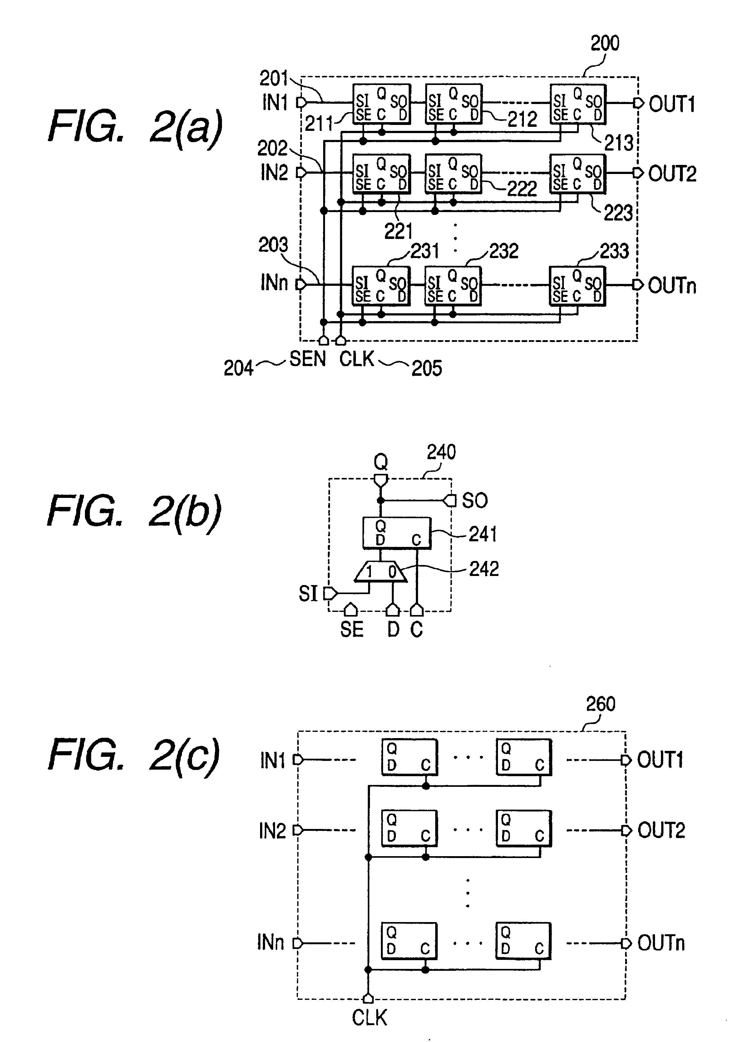
[0097]FIG. 16 shows the structure of a semiconductor integrated circuit having a test pattern generator according to this invention. The semiconductor integrated circuit 900 is composed of a test pattern generator 901 and a circuit under test (CUT) 902. The test pattern generator 901 has the same structure as the test pattern generator 800 shown in FIG. 15(a), where any combination of the relevant circuits mentioned above may be used for the identical pattern sequence generator 810 and the bit-flipping sequence generator 820. The circuit under test 902 may be either CUT 200 shown in FIG. 2(a) or CUT 260 as shown in FIG. 2(c). In this embodiment, neighborhood patterns which are valid for fault detection can be generated and thus a high fault coverage can be achieved with a smaller volume of test data.

third embodiment

[0098]FIG. 17 shows the structure of a semiconductor integrated circuit having a test pattern generator according to this invention. The semiconductor integrated circuit 920 is composed of plural test pattern generators 921 to 922 and a circuit under test (CUT) 923. Each of the test pattern generators 921 to 922 has the same structure as the test pattern generator 800, where any combination of the relevant circuits may be used for the identical pattern sequence generator 810 and the bit-flipping sequence generator 820. The circuit under test 923 may be either CUT 200 shown in FIG. 2(a) or CUT 260 as shown in FIG. 2(c). This embodiment offers not only the advantage of achieving a high fault coverage with a smaller volume of test data, but also another advantage that the overhead relating to wirings for scan chains in the CUT can be reduced by distribution of smaller size test pattern generators within the semiconductor integrated circuit.


PUM


Abstract

A semiconductor integrated circuit test method which reduces the required data volume for testing and efficiently detects faults in a circuit to be tested, the method comprising means 110 to generate identical pattern sequences repeatedly and means 120 to control flipped bits in pattern sequences, in order to generate neighborhood pattern sequences and use the neighborhood patterns to test the circuit under test 130. The neighborhood patterns include, in whole or in part, such pattern sequences as ones without flipped bits, ones with all or some flipped bits in one pattern and ones with all or some flipped bits in consecutive patterns or patterns at regular intervals, the interval being equivalent to a given number of patterns. Because a test pattern generator is provided independently of the circuit to be tested, the problem of a prolonged design period can be eliminated, a loss in the operating speed of the circuit under test is minimized and a high fault coverage can be achieved with less hardware overhead and a smaller volume of test data.

Description

FIELD OF THE INVENTION[0001]This invention relates to a semiconductor integrated circuit test method, and a test pattern generator and semiconductor integrated circuit which are used in the test method.BACKGROUND OF THE INVENTION[0002]Typical test methods for checking whether a semiconductor integrated circuit is acceptable or not are a stored test method and a built-in self-test method (BIST). In the stored test method, a test pattern for an assumed fault is obtained according to an algorithm and applied to the circuit to be tested through a test device which stores the pattern for comparison of response pattern from the circuit with an expected pattern. In the BIST method, the semiconductor integrated circuit incorporates a pseudo-random pattern generator and a signature analyzer to give a huge volume of pseudo-random patterns to the circuit to be tested and compare the compacted result of response pattern with an expected pattern.[0003]The stored test method has the following pro...

Claims


Application Information

Patent Timeline
Patent Type & Authority Patents(United States)
IPC IPC(8): G01R31/28G01R31/3183G11C29/04G11C29/10G06F11/22
CPCG01R31/3183G11C29/10G01R31/28
Inventor NAKAO, MICHINOBUHATAYAMA, KAZUMINATSUME, KOICHIROKIYOSHIGE, YOSHIKAZUKOUNO, MASAKIHAMAMOTO, MASATOYOSHIDA, HIDEFUMINAKAMURA, TOMOJI
Owner HITACHI LTD
Why Eureka
Try Eureka