Clip-type lead frame for source mounted die

Inactive Publication Date: 2005-08-02
INFINEON TECH AMERICAS CORP
View PDF11 Cites 6 Cited by
  • Summary
  • Abstract
  • Description
  • Claims
  • Application Information

AI Technical Summary

Benefits of technology

[0005]It would be very desirable to provide a very thin (low profile) surface mount package which lends itself to low cost manufacture, and which

Problems solved by technology

Advances in semiconductor processing technology, however, have made the parasit

Method used


Image

  • Clip-type lead frame for source mounted die
  • Clip-type lead frame for source mounted die
  • Clip-type lead frame for source mounted die

Examples


Embodiment Construction

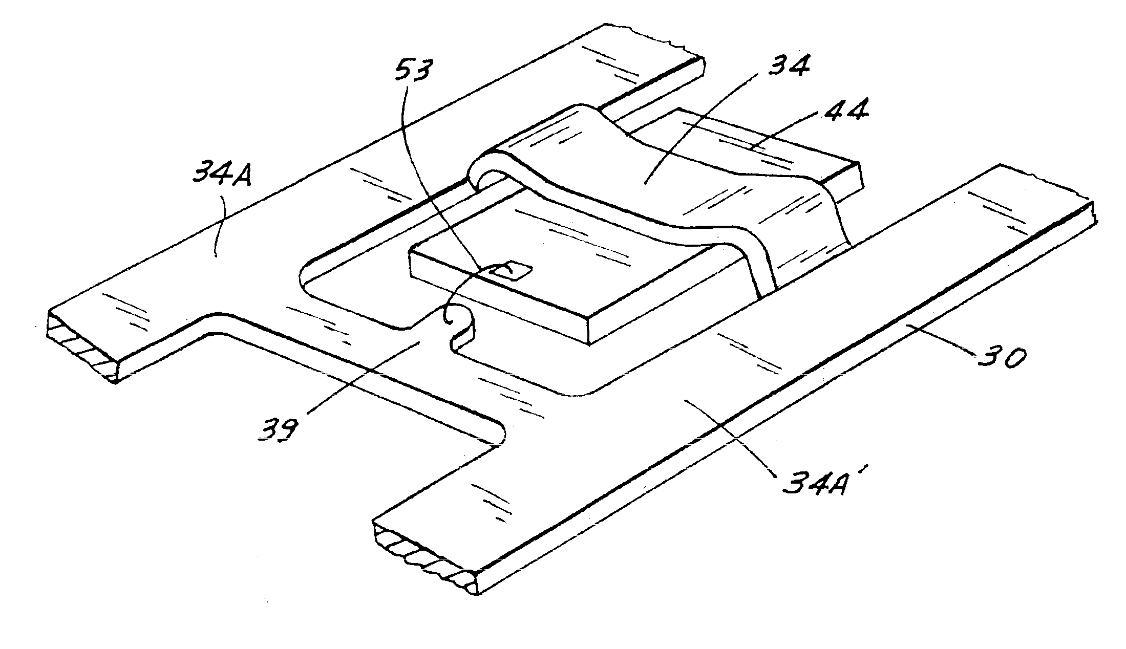
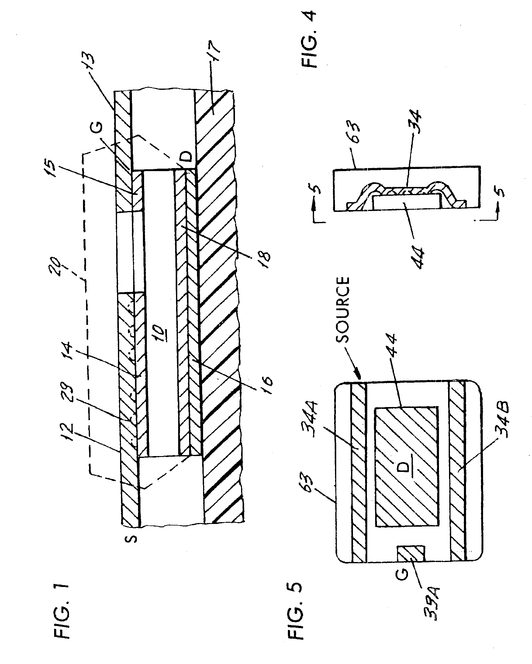
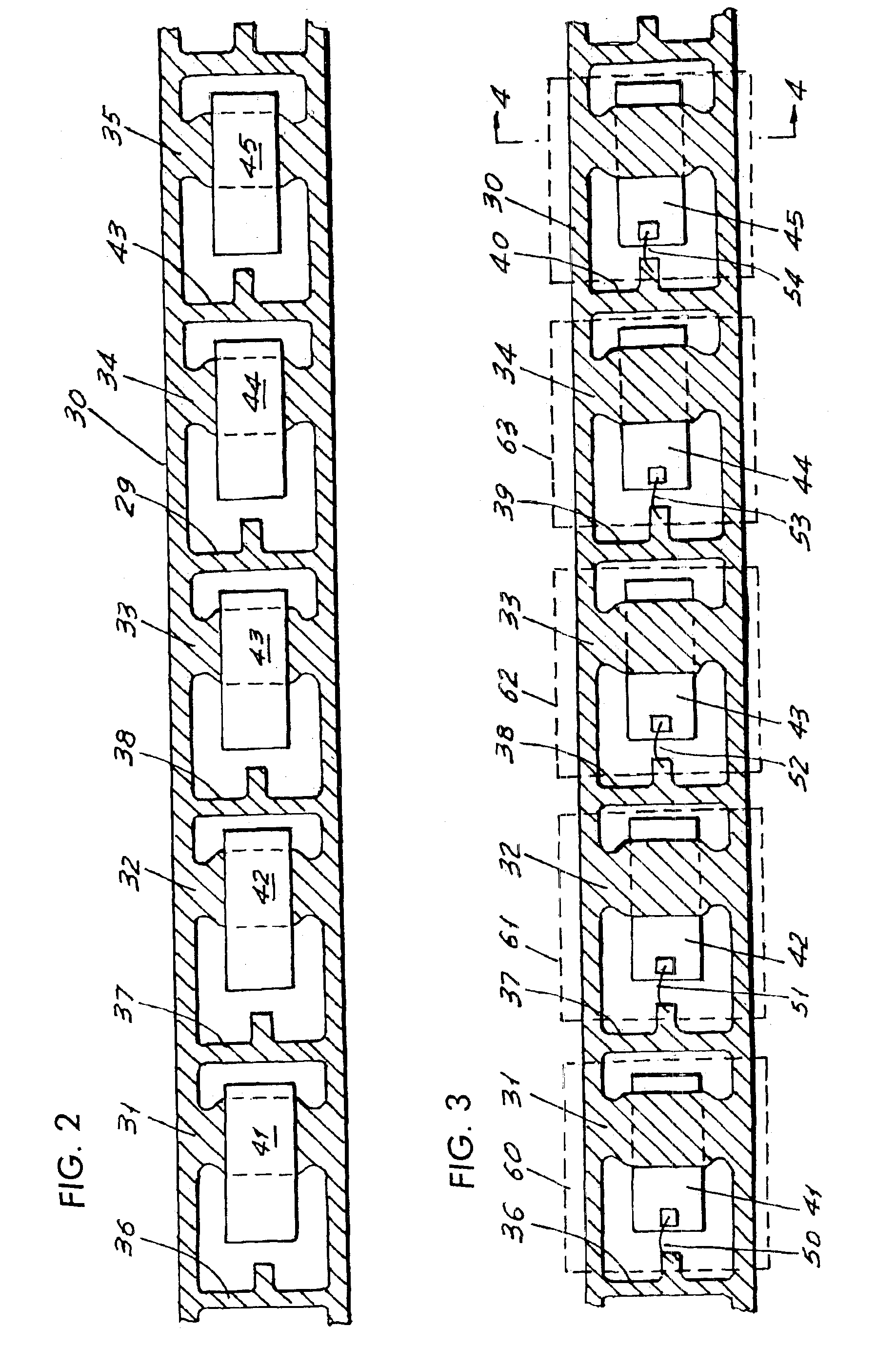
[0014]FIG. 1 shows one embodiment of a housing of the invention in which a semiconductor die 10 has a bottom power electrode such as a MOSFET drain (not shown) and a top power electrode such as a source electrode of a MOSFET on its opposite surface (not shown). The source and gate electrodes are connected to lead frame elements 12 and 13 as by a solder or conductive epoxy or by a polyamide adhesive tapes 14 and 15 respectively. If the source electrode is to be soldered to lead frame, it is possible to use solder-bump technology by providing an arrangement of solder bumps 29 either on the source electrode or an inner surface of the frame element 12. The bottom power electrode (or drain of a MOSFET) may be soldered or otherwise affixed to conductive trace 16 on printed circuit board 17 by a solder 18 or the like. A molded housing 20, shown in dotted lines is molded over and encapsulates the die 10 and its related lead frame elements. Significantly, the bottom of die 10 protrudes throu...


PUM


Abstract

A semiconductor package includes a lead frame having a displaced integral strap which is cupped out of a lead frame plane to provide a nest that receives a semiconductor chip electrically connected to an inner surface of the cupped strap. The semiconductor package further has a housing molded over and encapsulating the semiconductor chip with the frame such that a surface of the semiconductor chip facing away from the cupped strip is flush with or protrudes beyond a bottom of the housing.

Description

CROSS REFERENCE TO RELATED APPLICATION[0001]This is a divisional application of U.S. patent application Ser. No. 10 / 045,809, now U.S. Pat. No. 6,717,260 filed Jan. 11, 2002 in the names of Mark Pavier, Tim Sammon and Rachel Anderson and entitled A Clip-Type Lead Frame for Source Mounted Die which is based on and claims priority to U.S. Provisional Patent Application No. 60 / 263,137, filed Jan. 22, 2001, the entire disclosure of which is hereby incorporated by reference.FIELD OF THE INVENTION[0002]This invention relates to semiconductor device packages or housings and more specifically relates to a novel clip-type lead frame for a semiconductor device.BACKGROUND OF THE INVENTION[0003]Semiconductor devices, particularly power MOSFETs are frequently mounted on a conductive lead frame which is overmolded with an insulation housing. Leads extend from the lead frame through the housing for external connection to electrical circuits.[0004]Advances in semiconductor processing technology, how...

Claims


Application Information

Patent Timeline
IPC IPC(8): H01L23/495H01L23/48
CPCH01L23/49551H01L23/49562H01L2224/48247H01L2924/13091H01L24/48H01L2924/10253H01L2924/00H01L2224/05554H01L2224/05599H01L2224/45099H01L2224/85399H01L2924/00014H01L2224/45015H01L2924/207
Inventor PAVIER, MARKSAMMON, TIMANDERSON, RACHEL
Owner INFINEON TECH AMERICAS CORP
Why Eureka
Try Eureka